Interfacial Crosslinking for Efficient and Stable Planar TiO2 Perovskite Solar Cells
Abstract
The buried interface between the electron transport layer (ETL) and the perovskite layer plays a crucial role in enhancing the power conversion efficiency (PCE) and stability of n–i–p type perovskite solar cells (PSCs). In this study, the interface between the chemical bath deposited (CBD) titanium oxide (TiO2) ETL and the perovskite layer using multi‐functional potassium trifluoromethyl sulfonate (SK) is modified. Structural and elemental analyses reveal that the trifluoromethyl sulfonate serves as a crosslinker between the TiO2 and the perovskite layer, thus improving the adhesion of the perovskite to the TiO2 ETL through strong bonding of the ─CF3 and ─SO3 − terminal groups. Furthermore, the multi‐functional modifiers reduced interface defects and suppressed carrier recombination in the PSCs. Consequently, devices with a champion PCE of 25.22% and a fill factor (FF) close to 85% is achieved, marking the highest PCE and FF observed for PSCs based on CBD TiO2. The unencapsulated device maintained 81.3% of its initial PCE after operating for 1000 h.
Article type: Research Article
Keywords: electron transport layer, interface modification, perovskite layer, perovskite solar cell
Affiliations: Institute of Photoelectronic Thin Film Devices and Technology State Key Laboratory of Photovoltaic Materials and Cells Tianjin Key Laboratory of Efficient Solar Energy Utilization Ministry of Education Engineering Research Center of Thin Film Photoelectronic Technology Nankai University Tianjin 300350 China; Frontiers Science Center for New Organic Matter Nankai University Tianjin 300071 China; Haihe Laboratory of Sustainable Chemical Transformations Tianjin 300192 China
License: © 2024 The Author(s). Advanced Science published by Wiley‐VCH GmbH CC BY 4.0 This is an open access article under the terms of the http://creativecommons.org/licenses/by/4.0/ License, which permits use, distribution and reproduction in any medium, provided the original work is properly cited.
Article links: DOI: 10.1002/advs.202402796 | PubMed: 38961646 | PMC: PMC11434036
Relevance: Relevant: mentioned in keywords or abstract
Full text: PDF (2.1 MB)
Introduction
Organic–inorganic hybrid perovskite solar cells (PSCs) have garnered considerable attention in the photovoltaic industry due to their cost‐effective production and outstanding optoelectronic properties.[ ref. advs8467-bib-0001, ref. advs8467-bib-0002, ref. advs8467-bib-0003, ref. advs8467-bib-0004, ref. advs8467-bib-0005 ] Over the past decade, PSC technology has achieved a remarkable breakthrough in power conversion efficiency (PCE) of 26.1%, comparable to the highest‐performing single‐crystalline solar cells. These advancements position PSCs as having significant commercial potential. However, obstacles to PSC commercialization persist, such as stability and hysteresis effects.[ ref. advs8467-bib-0006, ref. advs8467-bib-0007, ref. advs8467-bib-0008, ref. advs8467-bib-0009, ref. advs8467-bib-0010, ref. advs8467-bib-0011, ref. advs8467-bib-0012, ref. advs8467-bib-0013 ]
In the general n‐i‐p structure, titanium oxide (TiO2) is commonly used as the electron transport layer (ETL) due to its suitable band energy level, low cost, and good thermal stability. The buried interfacial contact between the perovskite layer and ETL is crucial for the performance of PSCs.[ ref. advs8467-bib-0014, ref. advs8467-bib-0015, ref. advs8467-bib-0016, ref. advs8467-bib-0017 ] Photovoltaic performance parameters are closely linked to the interfacial charge transfer and transport ability. Efficient charge transfer and transport can lead to improved open circuit voltage (V oc), short circuit current density (J sc), and fill factor (FF).[ ref. advs8467-bib-0018, ref. advs8467-bib-0019, ref. advs8467-bib-0020 ] However, these processes will be significantly compromised in the presence of defects at the interfaces. Generally, the perovskite film surface contains a higher defect density compared to the bulk perovskite film, including uncoordinated Pb2+, I− and anti‐site defects PbI and IPb.[ ref. advs8467-bib-0012, ref. advs8467-bib-0021 ] As for the TiO2 ETL, there are oxygen and titanium vacancies, as well as anti‐site defects (TiO and OTi). All these defects at the heterojunction interface can create shallow and deep defect levels in the perovskite film and ETL, acting as recombination centers and leading to non‐radiative recombination in PSCs.[ ref. advs8467-bib-0022 ] In addition to impacting photovoltaic performance, these defects also influence the stability of PSCs. Perovskite crystals tend to collapse at defect sites, so reducing the defect density improves the stability of the perovskite film. Moreover, high electronic trap states in TiO2 ETL trigger undesirable charge accumulation and recombination, resulting in low PCE and significant hysteresis. Furthermore, O vacancies increase the catalytic activity of TiO2, leading to UV light instability and limiting the operational device lifetime.[ ref. advs8467-bib-0023, ref. advs8467-bib-0024 ]
Therefore, numerous researchers have concentrated on passivating interfacial defects by introducing functional materials. Modifying the surface of TiO2 is simple and effective in enhancing electron transport capability and adjusting energy level alignments, thereby improving device performance.[ ref. advs8467-bib-0001, ref. advs8467-bib-0009, ref. advs8467-bib-0014, ref. advs8467-bib-0017, ref. advs8467-bib-0025 ] For example, Tan et al. introduced PbCl2 to modify TiO2 surface. The resulting Cl‐capped TiO2 ETL displays suppressed anti‐site defects, leading to reduced interfacial recombination. Consequently, the PSCs exhibit a power PCE of 21.4% with negligible hysteresis.[ ref. advs8467-bib-0026 ] Kim et al. utilized Li‐doped mesoporous TiO2 with Li2CO3 to enhance electrical properties, resulting in an improved PCE from 23.15% to 25.28%.[ ref. advs8467-bib-0027 ] The introduction of Li salts reduced defects and optimized energy level alignments, benefiting carrier extraction and transport, consequently improving V oc and J sc. Additionally, Li et al. introduced organic ligands to regulate the crystal growth of TiO2 ETL through chemical bath deposition (CBD). These ligands also passivated the TiO2 surface, leading to an improved PCE of 24.8%.[ ref. advs8467-bib-0017 ] These studies underscore the significance of interfacial engineering in developing efficient PSCs.
In this study, we have developed a strategy that involves careful chemical selection to reduce interfacial defects in both the ETL and the perovskite layer using a cross‐linker. We chose potassium trifluoromethyl sulfonate (SK) to modify the chemical bath deposited TiO2 ETL. This strategy offers several potential benefits. First, the modifier at the interface enhances the adhesion of the perovskite with the oxide substrate through its two functional groups, resulting in a stable interfacial contact. Second, the ─CF3 and ─SO3 − groups could passivate the defects in the TiO2 ETL and perovskite film, respectively, which is advantageous for improving the photovoltaic performance of PSCs. Third, the K+ cation can also act as a growth‐controlling agent, leading to the formation of a uniform film with large crystal grains. The combined synergistic effects of these three factors contribute to improved PCE and long‐term stability of the device. Our work presents a new and general strategy for preparing high‐efficiency PSCs.
Result and Discussion
We deposited planar TiO2 as the ETL and treated it with a SK solution. The SK modification increased the wettability of the TiO2 as shown in Figure S1 (Supporting Information). The UV–vis absorption spectra and tauc‐plot curves are presented in Figure S2 (Supporting Information), corresponding to a bandgap of 3.015 eV for the control TiO2 and TiO2‐SK ETLs. The formamidinium lead iodide (FAPbI3) PSCs were fabricated using a one‐step method, and further details are presented in the experimental section. Figure advs8467-fig-0001 illustrates the electrostatic potential (ESP) distributions of the SK modifier. The SK agent exhibits distinctive positive and negative surface potential on the two sides of the molecule. Figure 1b shows a schematic diagram of the PSCs based on TiO2 ETL with the SK modifier. To comprehend the function of the SK modifier at the interface, we conducted Fourier transform infrared spectroscopy (FTIR) tests of the PbI2, SK, and PbI2‐SK mixtures (Figure 1c; Figure S3, Supporting Information). The results reveal that the stretching vibration of S═O is located at 1039.31 cm−1 for the SK sample, while the value shifted to 1033.10 cm−1 for the PbI2‐SK sample. Additionally, the stretching vibration of ─CF3 is located at 1165.44 cm−1 for the SK sample and shifted to 1179 cm−1. We further carried out the X‐ray photoelectron spectroscopy (XPS) of FAPbI3 and SK modified FAPbI3 perovskite films. The binding energy of F 1s increased from 687.05 to 688.70 eV while the binding energy of Pb 4f5/2 and Pb 4f7/2 reduced from 143.39 and 138.53 eV to 143.29 and 138.41 eV, respectively, as shown in Figure S4 (Supporting Information), indicating the interaction between the SK modifier and perovskite films. Due to the electron‐donating ability of the ─CF3 unit, the electron cloud density of F will decrease while the electron cloud density of Pb increases after accepting electrons from the ─CF3 units. Therefore, the binding energy of F inner shell electrons increased because of the weakened shielding effect of the outer electrons, leading to an increased binding energy of F 1s and a reduced binding energy of Pb 4f. Consequently, the ─SO3 − and ─CF3 units could act as Lewis‐base and tend to coordinate with the uncoordinated Pb2+, reducing defects in the perovskite film and charge recombination of the PSCs.[ ref. advs8467-bib-0015 ]
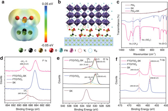
To investigate the interaction between the SK and TiO2 ETL, we performed XPS tests of the control TiO2 and SK treated TiO2 (TiO2‐SK) (Figure 1d–f; Figure S5, Supporting Information). Figure 1d shows the F 1s XPS spectrum, with the peak located at 687.05 eV for ─CF3 in the SK modifier. Due to the electron‐donating ability of ─CF3, the electron cloud density decreased after the interaction between the ─CF3 and TiO2, resulting in the increased binding energy of F 1s to 688.43 eV. In contrast, the electron density of Ti4+ increased after accepting electrons from ─CF3, leading to a slight decrease in the binding energy for Ti 2p1/2 and Ti 2p3/2 from 464.64 and 458.82 eV to 464.43 and 458.64 eV, respectively, as shown in Figure 1e. Figure 1f shows that the binding energy of O 1s for the SK sample is located at 532.67 eV. Meanwhile, the TiO2 ETL could be decoupled into two peaks, which are ascribed to the lattice oxygen (OL) and oxygen vacancy (OV), corresponding to a binding energy of O 1s at 529.95 and 531.36 eV.[ ref. advs8467-bib-0028 ] For TiO2‐SK ETL, the two peaks were shifted to 530.05 and 531.70 eV due to the occupation of the OV by the O atom of the ─SO3 − unit. Overall, both the aggregative negative potential of ─CF3 and the positive potential of ─SO3 − could coordinate with the vacancy in the TiO2 ETLs and perovskite layers due to its electron donating ability. As a result, the functional ─SO3 − and ─CF3 units of SK agents could modify the perovskite and TiO2 layer, acting as a crosslinker at the interface to improve the interfacial contact of the PSCs.
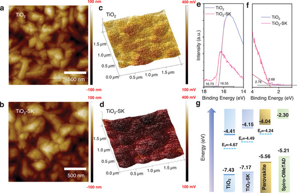
We further investigated the surface morphology of the TiO2 and TiO2‐SK ETLs using atomic force microscopy (AFM) and scanning electron microscopy (SEM) shown in Figure S6 (Supporting Information). A thin and compact TiO2 layer (≈30 nm) is deposited on the FTO substrates. The AFM results show that the root mean square roughness (RMS) of the TiO2 and TiO2‐SK ETLs is 37.7 and 32.9 nm, respectively, as depicted in Figure advs8467-fig-0002. Additionally, we utilized Kelvin probe force microscopy (KPFM) to measure the contact potential difference (CPD = Vtip − Vsample). The CPD images are shown in Figure 2c,d, and the CPD value of the TiO2 film decreased from 285 to 186 mV. These results indicate that TiO2‐SK ETL displays a reduced work function and an increased Fermi level. The strong interaction of SK with TiO2 alters the energy levels of the TiO2 ETL. To further assess the energy levels, ultraviolet photoelectron spectroscopy (UPS) tests were conducted (Figure S7 Supporting Information). The Ecutoff edge of the UPS spectra of the TiO2 shifted from 16.55 to 16.73 eV after modification with SK, as illustrated in Figure 2e,f, resulting in an elevated Fermi level from −4.67 to −4.49 eV, closer to that of the FAPbI3 film (Efermi = −4.24 eV). Consequently, the conduction band minimum (CBM) for TiO2 and TiO2‐SK were calculated to be −4.41 and −4.15 eV, respectively, which is beneficial for the energy level alignments between the ETL and perovskite film (CBM = −4.04 eV). Figure 2g illustrates the energy level alignments of the PSCs. The decreased energy level offset between the TiO2‐SK ETL and FAPbI3 perovskite film is advantageous for interfacial charge extraction and transfer, contributing to improved photovoltaic performance.
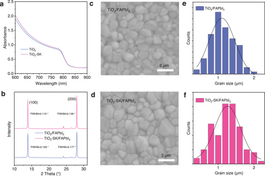
We then investigated the properties of the perovskite films. The FAPbI3 film, when using reference TiO2 and TiO2‐SK ETLs, was designated as TiO2/FAPbI3 and TiO2‐SK/FAPbI3, respectively. Both the TiO2/FAPbI3 and TiO2‐SK/FAPbI3 perovskite films exhibit the same absorption onset at 811 nm, corresponding to an optical bandgap of 1.52 eV, Figures advs8467-fig-0003 and S8 (Supporting Information). The TiO2‐SK/FAPbI3 perovskite film shows a slightly higher absorption coefficient compared to the TiO2/FAPbI3 perovskite film. The X‐ray diffraction patterns (XRD) of the TiO2/FAPbI3 and TiO2‐SK/FAPbI3 perovskite films reveal peaks at 13.92° (100) and 28.01° (200), as shown in Figure 3b. The full width at half maximum (FWHM) of the TiO2/FAPbI3 are 0.159 and 0.177, which is larger than that of 0.110 and 0.139 for TiO2‐SK/FAPbI3 perovskite films shown in Figure S9 (Supporting Information). The higher intensity of the characteristic peaks and smaller FWHM for TiO2‐SK/FAPbI3 perovskite film indicates better crystallinity. SEM was employed to investigate the morphology of perovskite films. From SEM images in Figures 3c,d and S10 (Supporting Information), it is evident that the TiO2‐SK/FAPbI3 perovskite film displays larger crystal grains compared to the TiO2/FAPbI3 perovskite film, mainly attributed to the K+ diffusion into the FAPbI3 film, promoting nucleation crystallization growth and enlarge the crystal size.[ ref. advs8467-bib-0014, ref. advs8467-bib-0025 ] The average grain size for the TiO2‐SK/FAPbI3 perovskite film is 1.3 µm, larger than the 1.1 µm for the TiO2/FAPbI3 perovskite film, as shown in Figure 3e,f. The increased grain size results in fewer defects, as the defects are generally distributed on the grain boundaries of the perovskite films.[ ref. advs8467-bib-0005 ] The improved morphology contributes to the enhancement of the photovoltaic performance of the PSCs.
To investigate the photovoltaic performance, we fabricated FAPbI3 PSCs using a device configuration of FTO/c‐TiO2/perovskite/Spiro‐OMeTAD/Au, and the experimental details are provided in the Experimental Section. Figures advs8467-fig-0004 and S11 (Supporting Information) illustrate the photovoltaic performance of the TiO2‐SK PSCs compared to that of the control TiO2 PSCs, with detailed parameters displayed in Table S1 (Supporting Information). Notably, significant improvements are observed in the V oc and FF, which improved from 1.13 ± 0.05 V to 1.16 ± 0.05 V and 82.5 ± 1.0% to 84.0 ± 0.9%, respectively. Additionally, Figure 4b presents the current density–voltage (J–V) curves of the champion devices. The TiO2‐SK PSC exhibits a remarkable reverse scanning PCE of 25.22% with a V oc of 1.165 V, a J sc of 25.51 mA cm−2 and an FF of 84.9%. The forward scanning PCE is 24.80% with a V oc of 1.161 V, a J sc of 25.50, and an FF of 83.8%. Due to enhanced carrier extraction ability and suppressed nonradiative recombination, the TiO2‐SK PSC displays less hysteresis. In contrast, the control PSC shows a reverse scanning PCE of 24.01% with a V oc of 1.130 V, a J sc of 25.47 mA cm−2 and an FF of 83.5%, while the forward scanning PCE is 22.04% with a V oc of 1.11 V and a J sc of 25.44 mA cm−2 and an FF of 78.1%. Furthermore, Figure 4c displays the stabilized power outputs (SPO) of the TiO2 and TiO2‐SK PSCs, corresponding to the PCEs of 23.51% and 24.82%. External quantum efficiency (EQE) measurements were performed to ascertain the J sc value, resulting in integrated J sc values of 24.85 mA cm−2 for the control TiO2 PSC and 24.91 mA cm−2 for the TiO2‐SK PSC, as shown in Figure 4d.
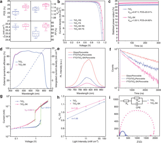
To investigate the carrier extraction and transport ability of the TiO2 and TiO2‐SK, we conducted steady‐state photoluminescence (PL) and time‐resolved photoluminescence (TRPL) tests. The PL results indicate an emission peak at ≈ 810 nm, as shown in Figure 4e,f, and the FAPbI3‐SK film displays lower PL intensity compared to the FAPbI3 film due to enhanced charge transfer from the perovskite layer to the TiO2 ETL. This result was further confirmed by the TRPL test, which revealed faster PL quenching for TiO2‐SK/FAPbI3 film, verifying a shorter carrier lifetime of 761.7 ns compared to 1142.6 ns for the TiO2/FAPbI3 film (Table S2 Supporting Information). The reduced lifetime indicates efficient electron extraction at the TiO2‐SK ETL/perovskite interface with SK modification, thereby reducing charge accumulation at the interface and suppressing device hysteresis. To quantify the trap defect density of the perovskite films, we conducted space‐charge limited current (SCLC) tests on the electron‐only devices in a structure of FTO/TiO2/Perovskite/PCBM/BCP/Au (Figure 4g). The Vtfl values were estimated to be 0.934 and 1.812 V, respectively. The trap density was calculated using the equation Ntrap = 2ɛrɛ0VTFL/eL2, where e represents the elementary charge, and ɛr and ɛ0 are the relative dielectric constant and vacuum permittivity, respectively.[ ref. advs8467-bib-0029, ref. advs8467-bib-0030 ] The trap densities of the TiO2 and TiO2‐SK PSCs were estimated to be 2.96 × 10¹⁶ and 1.51 × 10¹⁶.[ ref. advs8467-bib-0031 ]
The relationship between V oc and light intensity was also analyzed, as depicted in Figure 4h. Linear fitting of V oc versus log‐scaled light intensity allows the reflection of trap‐assisted recombination through the slope value and nkT/q (where k represents the Boltzmann constant, T is temperature, q is the electric charge, and n is the ideality factor). The smaller ideality factor of 1.44 for the TiO2 PSC compared to 1.68 for the TiO2‐SK PSC indicates a suppressed trap‐assisted recombination. Furthermore, electrical impedance spectroscopy (EIS) measurements were conducted to further investigate the interfacial charge transport behavior in PSCs (Figure 4i; Table S3, Supporting Information). The increased recombination resistance (Rrec = 1898 Ω) for TiO2‐SK PSC indicates suppressed carrier recombination compared to the TiO2 PSC (Rrec = 349 Ω). Additionally, the decreased transport resistance (Rtr) for the TiO2‐SK PSC (13.78 Ω vs 15.05 Ω for TiO2 PSC) is beneficial for the charge transport, resulting in an improved FF and reducing hysteresis.[ ref. advs8467-bib-0032, ref. advs8467-bib-0033 ]
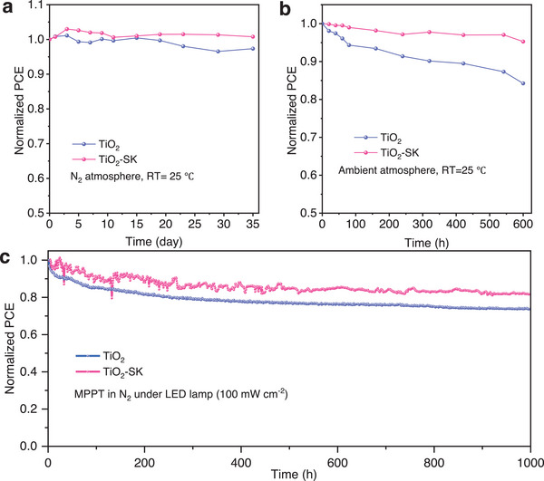
We assessed the stability of the PSCs by storing them in an N2 atmosphere, and the results are presented in Figures advs8467-fig-0005 and S12 (Supporting Information). The TiO2‐SK PSC retained almost 100% of their initial PCE for 35 days, while the control device decreased to 97%. Additionally, we tested the stability of the unencapsulated PSCs in ambient conditions (RH = 20 ± 5%, RT = 25 ± 5 °C), and found that the TiO2 and TiO2‐SK PSCs preserved 84% and 95% of the initial efficiency, respectively, as shown in Figure 5b and Figure S13 (Supporting Information). Furthermore, we investigated the operational stability of the PSCs by aging the unencapsulated devices under a nitrogen atmosphere, using maximum power point (MPP) tracking under an LED lamp (light intensity 100 mw cm−2). Figure 5c shows that the normalized PCE of the TiO2 PSC decreased to 73.7%, while the TiO2‐SK PSC remained at 81.3% of the initial efficiency after operating for 1000 h. The improved stability of the TiO2‐SK PSCs is attributed to the reduced interfacial defect density and improved energy level alignments after interfacial cross‐linking modification. The reduction in recombination and charge accumulation during the charge transfer process contributes to the operational stability of the PSCs under light illumination.[ ref. advs8467-bib-0021, ref. advs8467-bib-0034, ref. advs8467-bib-0035 ] Moreover, the high crystallinity and enlarged grain size resulting from K‐doping also contribute to better stability and photovoltaic performance of the TiO2‐SK PSCs.
Conclusion
In summary, our introduction of multi‐functional SK modifier has led to improvements in both the power conversion efficiency and stability of the PSCs. The two terminal groups ─SO3 − and ─CF3 can interact with the TiO2 ETL and perovskite layer through ionic and hydrogen bonds, thereby strengthening the adhesion between the TiO2 ETL and perovskite layer. This interaction also reduces interfacial defects and minimizes the non‐radiative recombination of the PSCs. Furthermore, the SK modifier improves the morphology and enlarges the grain size of the perovskite film, which contributes to a reduced defect density and prolonged carrier lifetime of the perovskite film. In addition, the modification adjusts the energy level alignments of the TiO2 ETL and perovskite layer, which is beneficial for interfacial charge transfer, thereby reducing the charge accumulation at the TiO2/perovskite interface. As a result, the FAPbI3 PSCs display an improved V oc and FF close to 85%. In conclusion, we achieved a champion PCE of 25.22% with negligible hysteresis and excellent operational stability. Our work provides a straightforward method to fabricate efficient and stable FAPbI3 PSCs.
Conflict of Interest
The authors declare no conflict of interest.
Author Contributions
J.L. designed the experiment and supervised the study. L.D. conducted the device fabrication, characterization, and manuscript preparation. S.L. participated in the SCLC and FTIR tests. X.W. contributed to the ESP analysis. Z.Z. conducted the EIS tests. L.D. and J.L. wrote the manuscript. All authors discussed the results and contributed to the manuscript revision.
Supplementary Materials
References
- 1 J. J. Yoo , G. Seo , M. R. Chua , T. G. Park , Y. Lu , F. Rotermund , Y. K. Kim , C. S. Moon , N. J. Jeon , J. P. Correa‐Baena , V. Bulovic , S. S. Shin , M. G. Bawendi , J. Seo , Nature. 2021, 590, 587.33627807
- 2 J. Park , J. Kim , H. S. Yun , M. J. Paik , E. Noh , H. J. Mun , M. G. Kim , T. J. Shin , S. I. Seok , Nature. 2023, 616, 724.36796426
- 3 Y. Zhao , K. Zhu , Chem. Soc. Rev. 2016, 45, 655.26645733
- 4 Q. Jiang , L. Zhang , H. Wang , X. Yang , J. Meng , H. Liu , Z. Yin , J. Wu , X. Zhang , J. You , Nat. Energy. 2016, 2, 16177.
- 5 Q. Jiang , Y. Zhao , X. Zhang , X. Yang , Y. Chen , Z. Chu , Q. Ye , X. Li , Z. Yin , J. You , Nat. Photonics. 2019, 13, 460.
- 6 D. H. Kang , N. G. Park , Adv. Mater. 2019, 31, 1805214.
- 7 Y. Rong , Y. Hu , S. Ravishankar , H. Liu , X. Hou , Y. Sheng , A. Mei , Q. Wang , D. Li , M. Xu , J. Bisquert , H. Han , Environ Sci. 2017, 10, 2383.
- 8 S. A. L. Weber , I. M. Hermes , S.‐H. Turren‐Cruz , C. Gort , V. W. Bergmann , L. Gilson , A. Hagfeldt , M. Graetzel , W. Tress , R. Berger , Environ Sci. 2018, 11, 2404.
- 9 M. Kim , J. Jeong , H. Lu , T. K. Lee , F. T. Eickemeyer , Y. Liu , I. W. Choi , S. J. Choi , Y. Jo , H. B. Kim , S. I. Mo , Y. K. Kim , H. Lee , N. G. An , S. Cho , W. R. Tress , S. M. Zakeeruddin , A. Hagfeldt , J. Y. Kim , M. Gratzel , D. S. Kim , Science. 2022, 375, 302.35050659
- 10 L. Duan , H. Zhang , M. Liu , M. Grätzel , J. Luo , ACS Energy Lett. 2022,7, 2911.
- 11 Z. Wang , L. Zeng , T. Zhu , H. Chen , B. Chen , D. J. Kubicki , A. Balvanz , C. Li , A. Maxwell , E. Ugur , R. Dos Reis , M. Cheng , G. Yang , B. Subedi , D. Luo , J. Hu , J. Wang , S. Teale , S. Mahesh , S. Wang , S. Hu , E. Jung , M. Wei , S. M. Park , L. Grater , E. Aydin , Z. Song , N. J. Podraza , Z. H. Lu , J. Huang , et al., Nature. 2023, 618, 74.36977463
- 12 H. Wang , Z. Wang , Z. Yang , Y. Xu , Y. Ding , L. Tan , C. Yi , Z. Zhang , K. Meng , G. J. A. M. Chen , Adv. Mater. 2020, 32, 2000865.
- 13 Z. Zhang , H. Wang , T. J. Jacobsson , J. Luo , Nat. Commun. 2022, 13, 7639.36496471
- 14 Y. Dong , W. Shen , W. Dong , C. Bai , J. Zhao , Y. Zhou , F. Huang , Y. B. Cheng , J. Zhong , Adv. Energy Mater. 2022, 12, 2200417.
- 15 C. Zheng , L. Liu , Y. Li , A. Gao , Z. Yang , L. Zhang , Z. Liu , D. Wang , S. Liu , Adv. Energy Mater. 2023, 13, 2301302.
- 16 C. Luo , G. Zheng , F. Gao , X. Wang , C. Zhan , X. Gao , Q. Zhao , Nat. Photonics. 2023, 17, 856.
- 17 H. Huang , P. Cui , Y. Chen , L. Yan , X. Yue , S. Qu , X. Wang , S. Du , B. Liu , Q. Zhang , Z. Lan , Y. Yang , J. Ji , X. Zhao , Y. Li , X. Wang , X. Ding , M. Li , Joule. 2022, 6, 2186.
- 18 H. Guo , W. Xiang , Y. Fang , J. Li , Y. Lin , Angew Chem Int Ed Engl. 2023, 62, 202304568.
- 19 W. Dong , C. Zhu , C. Bai , Y. Ma , L. Lv , J. Zhao , F. Huang , Y.‐B. Cheng , J. Zhong , Angew. Chem., Int. Ed. 2023, 62, 2023025.
- 20 H. Wang , Z. Zhang , J. V. Milić , L. Tan , Z. Wang , R. Chen , X. Jing , C. Yi , Y. Ding , Y. Li , Y. Zhao , X. Zhang , A. Hagfeldt , M. Grätzel , J. Luo , Adv. Energy Mater. 2021, 11, 2101082.
- 21 B. Chen , P. N. Rudd , S. Yang , Y. Yuan , J. Huang , Chem. Soc. Rev. 2019, 48, 3842.31187791
- 22 W. Hu , S. Yang , S. Yang , Trends in Chemistry. 2020, 2, 148.
- 23 W. Li , W. Zhang , S. Van Reenen , R. J. Sutton , J. Fan , A. A. Haghighirad , M. B. Johnston , L. Wang , H. J. Snaith , Environ Sci. 2016, 9, 490.
- 24 C. F. J. Lau , Z. P. Wang , N. Sakai , J. H. Zheng , C. H. Liao , M. Green , S. J. Huang , H. J. Snaith , A. Ho‐Baillie , Adv. Energy Mater. 2019, 9, 1901685.
- 25 M. J. Jeong , C. S. Moon , S. Lee , J. M. Im , M. Y. Woo , J. H. Lee , H. Cho , S. W. Jeon , J. H. Noh , Joule. 2022, 7, 1.
- 26 H. Tan , A. Jain , O. Voznyy , X. Lan , F. P. Garcia de Arquer , J. Z. Fan , R. Quintero‐Bermudez , M. Yuan , B. Zhang , Y. Zhao , F. Fan , P. Li , L. N. Quan , Y. Zhao , Z. H. Lu , Z. Yang , S. Hoogland , E. H. Sargent , Science. 2017, 355, 722.28154242
- 27 M. Kim , I.‐W. Choi , S. J. Choi , J. W. Song , S.‐I. Mo , J.‐H. An , Y. Jo , S. Ahn , S. K. Ahn , G.‐H. Kim , D. S. Kim , Joule. 2021, 5, 659.
- 28 G. Ou , Y. Xu , B. Wen , R. Lin , B. Ge , Y. Tang , Y. Liang , C. Yang , K. Huang , D. Zu , R. Yu , W. Chen , J. Li , H. Wu , L.‐M. Liu , Y. Li , Nat. Commun. 2018, 9, 1302.29615620
- 29 V. M. Le Corre , E. A. Duijnstee , O. El Tambouli , J. M. Ball , H. J. Snaith , J. Lim , L. J. A. Koster , ACS Energy Lett. 2021, 6, 1087.33869770
- 30 R. H. Bube , J. Appl. Phys. 1962, 33, 1733.
- 31 T. S. Su , F. T. Eickemeyer , M. A. Hope , F. Jahanbakhshi , M. Mladenovic , J. Li , Z. Zhou , A. Mishra , J. H. Yum , D. Ren , A. Krishna , O. Ouellette , T. C. Wei , H. Zhou , H. H. Huang , M. D. Mensi , K. Sivula , S. M. Zakeeruddin , J. V. Milic , A. Hagfeldt , U. Rothlisberger , L. Emsley , H. Zhang , M. Gratzel , J. Am. Chem. Soc. 2020, 142, 19980.33170007
- 32 X. Chu , Q. Ye , Z. Wang , C. Zhang , F. Ma , Z. Qu , Y. Zhao , Z. Yin , H.‐X. Deng , X. Zhang , J. You , Nat. Energy. 2023, 8, 372.
- 33 Q. Tan , Z. Li , G. Luo , X. Zhang , B. Che , G. Chen , H. Gao , D. He , G. Ma , J. Wang , J. Xiu , H. Yi , T. Chen , Z. He , Nature. 2023, 620, 545.37224876
- 34 Z. Zeng , J. Zhang , X. Gan , H. Sun , M. Shang , D. Hou , C. Lu , R. Chen , Y. Zhu , L. Han , Adv. Energy Mater. 2018, 8, 1801050.
- 35 C. Li , A. Guerrero , S. Huettner , J. Bisquert , Nat. Commun. 2018, 9, 5113.30504825