Two-Dimensional Hybrid Composites of SnS2 Nanosheets Array Film with Graphene for Enhanced Photoelectric Performance
Abstract
Two-dimensional (2D) metal dichalcogenides have attracted considerable attention for use in photoelectric devices due to their unique layer structure and strong light-matter interaction. In this paper, vertically grown SnS2 nanosheets array film was synthesized by a facile chemical bath deposition (CBD). The effects of deposition time and annealing temperature on the quality of SnS2 films was investigated in detail. By optimizing the preparation conditions, the SnS2 array film exhibited efficient photoelectric detection performance under sunlight. Furthermore, in order to improve the performance of the photodetector based on SnS2 nanosheets film, a transparent graphene film was introduced as the hole-transport layer by wet-chemical method directly transferring techniques. Graphene/SnS2 nanosheets array film heterojunction photodetectors exhibit enhanced photoresponsivity. The light on/off ratio of the photodetector based on graphene/SnS2 was 1.53, about 1.4 times higher than that of the pristine SnS2 array films. The improved photoresponse performance suggested that the effective heterojunction between vertical SnS2 nanosheets array film and graphene suppresses the recombination of photogenerated carriers. The results indicate that the graphene/SnS2 heterojunction photodetectors have great potential in photodetection devices.
Article type: Research Article
Keywords: graphene/SnS, charge separation, photodetectors
Affiliations: SZU-NUS Collaborative Innovation Center for Optoelectronic Science & Technology, International Collaborative Laboratory of 2D Materials for Optoelectronics Science and Technology of Ministry of Education, College of Optoelectronic Engineering, Shenzhen University, Shenzhen 518060, China; College of Electronic Science and Technology, Shenzhen University, Shenzhen 518060, China; School of Physics and Telecommunication Engineering, South China Normal University, Guangzhou 510006, China; Key Laboratory of Material Physics of Ministry of Education, School of Physics and Engineering, Zhengzhou University, Zhengzhou 450052, China
License: © 2019 by the authors. CC BY 4.0 Licensee MDPI, Basel, Switzerland. This article is an open access article distributed under the terms and conditions of the Creative Commons Attribution (CC BY) license (http://creativecommons.org/licenses/by/4.0/).
Article links: DOI: 10.3390/nano9081122 | PubMed: 31382642 | PMC: PMC6723453
Relevance: Relevant: mentioned in keywords or abstract
Full text: PDF (2.2 MB)
1. Introduction
The unique physical and chemical properties of graphene has inspired the exploration of two-dimensional (2D) materials [ref. 1]. Graphene has a huge electrical mobility that approaches 200,000 cm2 V−1 s−1 and is used for electrons and hole free sheets [ref. 2]. Moreover, the absorption of a single-layer graphene is ~2.3% over a broad wavelength range [ref. 3]. As a result, graphene has been used in many electronic and optoelectronic fields, including mode-locked lasers [ref. 4,ref. 5], photodetectors [ref. 6,ref. 7,ref. 8], transistors [ref. 9,ref. 10], batteries [ref. 11], photovoltaics [ref. 12], photocatalysis [ref. 13,ref. 14], and so forth. Among these applications, photodetectors are critical optoelectronic components that convert optical radiation into electrical signal [ref. 15,ref. 16] and they have been widely used in medical analysis, astronomy [ref. 17], environmental sensing [ref. 18], and optical communication [ref. 19,ref. 20], However, single-layer graphene itself is a band-free Dirac semi-metal, which limits its application in optoelectronic devices where semiconducting properties are required [ref. 21].
Recently, the combination of graphene with various two-dimensional (2D) layered materials has proven to be an effective strategy to achieve the unique electronic and optoelectronic applications of 2D materials [ref. 22,ref. 23,ref. 24]. Among the various kinds of 2D layered metal dichalcogenides, SnS2 is an n-type semiconductor with a layered cadmium iodide (CdI2) structure. Each layer is covalently bonded by three atomic planes and separated by weak van der Waals interaction. SnS2 exhibits a high optical absorption coefficient and strong photoconductive properties in visible regions and this has given rise to increased interest due to its particular structure, suitable band gap (~2.2 eV), good chemical stability, low-cost and environmental friendliness [ref. 25]. Therefore, it has been widely used in many fields, such as lithium (sodium) ion batteries [ref. 26,ref. 27], solar cells [ref. 28,ref. 29], photocatalysis [ref. 30,ref. 31], field effect transistors [ref. 32,ref. 33], photodetectors [ref. 34,ref. 35,ref. 36], etc. Su et al. [ref. 37] used chemical vapor deposition (CVD) to introduce metal seeds on the substrate to achieve high-quality SnS2 thin film for location-selective synthesis, and the response time and quantum efficiency of the fabricated photodetector was ~5 microseconds and 11.3%, respectively. Tao et al. [ref. 38] studied a transparent polypropylene (PP) film flexible photodetector based on SnS2 self-assembled microsphere film by double-sided tape. The device shows a good photoresponse in the region of UV (300 nm) though to NIR (830 nm) light. However, vertical SnS2 nanosheets array film combined with transparent graphene film for photodetector application has rarely been investigated.
In this work, SnS2 film vertically grown on conductive fluorine-doped tin oxide (FTO) glass substrate was fabricated by the low-temperature CBD method. The optimal fabrication conditions for pure SnS2 array film was investigated. After annealing treatment at 300 °C in nitrogen atmosphere, the crystalline of SnS2 showed an obvious improvement. A highly transparent graphene thin film was deposited onto n-type SnS2 array film to form a Schottky junction. The graphene/SnS2 heterojunction was constructed by the direct wet-chemical transfer method. Graphene, as a hole-transport layer, promotes the charge transfer at the interface of the heterojunction. The corresponding photodetector based on graphene/SnS2 composite film shows enhanced and stable photoelectric performance.
2. Experimental Methods
2.1. Synthesis of SnS2 Nanosheets Array Film
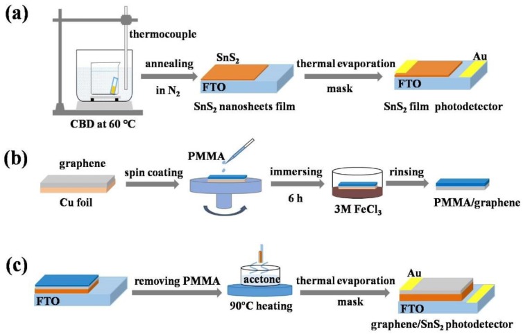
All chemicals in the experiment were of the highest purity available and were used without further purification. In this experiment, the resistivity of distilled water was 18.0 M Ω cm. FTO substrates were ultrasonically cleaned successively with acetone, isopropanol, and ethanol, followed by rinsing with deionized water and drying in the flow of N2. The cleaned substrates were further treated by plasma for 5 min. SnS2 nanosheets array film was synthesized by the CBD method, similar to that previously reported in [ref. 39]. The synthesized process of the SnS2 film is shown in Figure 1a. Briefly, 10 mol of SnCl4·5H2O (Aladdin, 99.995% metals basis, Shanghai, China) was dissolved in 240 mL anhydrous ethanol. The mixture was stirred for 15 min under ambient conditions before 0.15 mol thioacetamide (CH3CSNH2, Aladdin, Shanghai, China) was added. Then, the mixture was placed in a beaker of 50 mL volume. Finally, a piece of cleaned FTO substrate was placed at an angle against the wall of the beaker with the conductive side facing down. The CBD process was carried out at 60 °C in a water bath kettle for 0.5 h, 1 h and 1.5 h, respectively. When the kettle was cooled down to room temperature, the FTO substrates were removed and thoroughly rinsed with deionized water. Finally, the samples were dried in an oven at 80 °C for 6 h. To further remove any impurities on the sample surface and improve the crystallinity, the samples were annealed at 250 °C, 300 °C and 350 °C for 1 h in nitrogen (N2) atmosphere [ref. 40,ref. 41]. The prepared samples were dried and cleaned in ambient conditions for further characterization.
2.2. Preparation of Graphene/SnS2 Heterojunction
Graphene/SnS2 heterojunction was constructed by the wet-chemical transfer method [ref. 42,ref. 43], where the graphene layer was directly transferred onto SnS2 film. The large area of graphene films on Cu foil substrates were purchased from the Graphene Technology Corporation, China. Firstly, graphene film was delaminated from the Cu foil by the conventional polymethyl methacrylate (PMMA, Aladdin, ACS, Shanghai, China) assisted transfer method (as shown in Figure 1b) [ref. 44]. PMMA was spin-coated onto the graphene film at 2000 r/min. The PMMA/graphene/Cu foils was dried at 100 °C for 3 min, then the samples were placed in 3 M FeCl3 ((Aladdin, ACS, Shanghai, China) solution for 6 h to etch the Cu foil completely. The floating PMMA/graphene films were fished out and rinsed several times in deionized water. Finally, the PMMA/graphene film was picked up by FTO substrates with SnS2 nanosheets grown and dried in a flow of N2, as shown in Figure 1c. Subsequently, the whole sample was treated by acetone vapors to dissolve the PMMA by heating the acetone solution to 90 °C. The obtained graphene/SnS2 heterojunction films were then used for photodetector fabrication.
2.3. Characterization
The morphology and microstructure of the samples were characterized by field emission scanning electron microscope (SEM) (Hitachi, Tokyo, Japan, SU8010 (MDTC-EQ-M18-01)). The composition of the crystal structure was identified by X-ray diffractometer (Rigaku, Ultima IV, Tokyo, Japan) using Cu Kα radiation (λ = 1.5418Å). UV-vis absorption was recorded with Cary 5000 UV-Vis-NIR spectrophotometer (Agilent Technologies, CA, USA) in the range of 350 nm to 800 nm. In order to investigate the photoelectric performance of the samples, Au electrodes were deposited on the samples with a shadow mask by a thermal evaporation method. The photoelectric performance of the photodetector based on the pristine SnS2 and graphene/SnS2 thin films was investigated by an electrochemical workstation (CH Instruments, model CHI 760E, Austin, TX, USA). The CHI electrochemical workstation was used to measure dark and illuminated current at a scan rate of 10 mV/s. The bias voltage was 3 V. The active area of samples was kept at 1 cm2 by a mask. A 500W xenon lamp was used to simulate sunlight. (Spectra Physics, CA, USA).
3. Results and Discussion
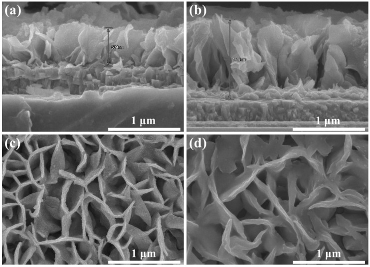
The vertically grown SnS2 array films on FTO substrate were prepared by a simple CBD method (see Experimental Methods). We investigated the density change of SnS2 nanosheets by changing the reaction time to obtain the optimal condition. The reaction temperature of all the samples was 60 °C. Altering the reaction time from 1 h to 1.5 h barely changed the morphology of the nanocrystalline, but the thickness of the single SnS2 nanosheets film increased from 534 nm to 1120 nm, as shown in Figure 2a,b. The SnS2 nanocrystals with non-overlapping structures were interlaced and interconnected with each other. With the extension of the reaction time, the density of ordered SnS2 gradually increased when the CBD time was between 0.5 h and 1 h. The top-view SEM image of pristine SnS2 film on FTO prepared at 60 °C for 0.5 h is shown in Figure S1 (Supplementary Materials). However, when the CBD time exceeds 1 h, the film density decreased due to the curing mechanism of the reaction (the corresponding top-view SEM images are shown in Figure 2c,d). Therefore, the optimal condition for CBD is 1 h. The effect of annealing conditions on the film density will be further explored in future work. We also measured the surface roughness of the pristine SnS2 and graphene/ SnS2 thin film on FTO prepared at 60 °C for 1 h and the AFM results are presented in Figure S2a,b (Supplementary Materials). According to the AFM results, compared with pristine SnS2, the average surface roughness of graphene/SnS2 thin film decreased from 70 nm to 45.7 nm. The results show that the sample with lower surface roughness and better compactness is prepared under this condition. In our experiment, an orange film started to peel off from the FTO substrate when the reaction time was longer than 1.5 h. The reason for the dissolution/partial peel-off might be explained by considering the reaction kinetics [ref. 45]. As the reaction time increases, the concentration of reactants in the solution decreases. When the concentration of reactants near the FTO substrate is lower than the concentration allowed by the chemical equilibrium, an opposite reaction will occur to dissociate the membrane to make up for the deficiency, which accounts for the film peel-off.
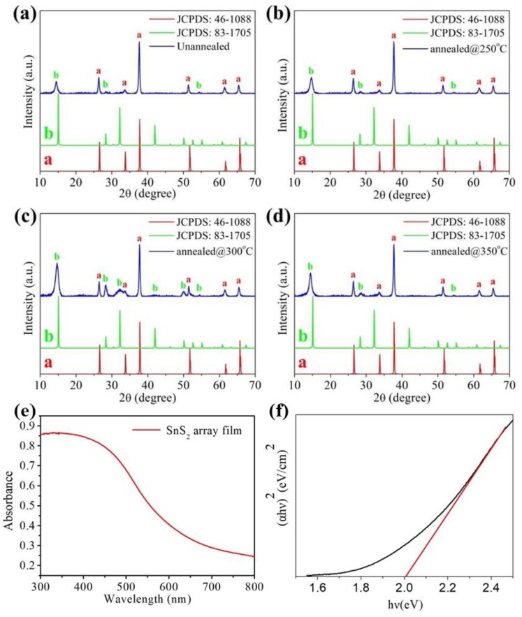
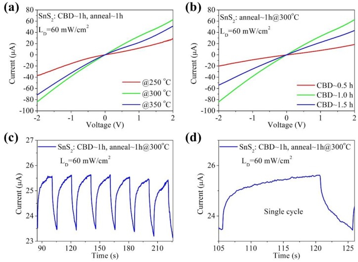
The crystallinity of SnS2 array films was characterized by X-ray diffraction. Figure 3 displays the XRD patterns of prepared samples fabricated at 60 °C and annealed at 250, 300 and 350 °C for 1 h in N2 atmosphere. The red curves in Figure 3 are the diffraction peaks of FTO substrate (JCPDS No. 46-1088). All of the diffraction peaks can be indexed according to the standard hexagonal structure of SnS2 (JPCDS No. 83-1705; space group: P/3ml (no.164); a = 0.3638 nm, c = 0.588 nm). The XRD diffraction peaks at 14.83°, 28.45°, 32.14° correspond to the (001), (100), (002) planes of the samples. No other peaks were observed in the XRD spectra at other angles, which suggests the high purity of the SnS2 films. The investigation also showed that no phase transition occurs during the calcining process. In addition, we used the Scherrer equation to estimate the thickness of the individual sheets that are standing up perpendicular to the substrate in the XRD data. For example, the full width at half maximum (FHWM) of the prepared samples fabricated at 60 °C for a CBD time of 1 h are 0.6217, 0.6827, 0.7382 degrees, which correspond to the XRD diffraction peaks at 14.83°, 28.45°, 32.14°, respectively. According to the Scherrer equation, the average grain thickness is 12.89 nm. Similarly, the average grain thickness of samples for 1.5 h is 14.13 nm. The data shows that the average thickness increases with the increasing reaction time. By increasing annealed temperature (Figure 3a–c), it is interesting to note that the intensity of the (100) and (002) diffraction peaks of the SnS2 was significantly enhanced as the annealing temperature increased, except for the sample annealed at 350 °C (Figure 3d), which indicates that the higher temperature is beneficial to obtain high crystalline samples. When the temperature of the annealing treatment increased to 350 °C, the relative intensity of the (002) diffraction peak decreased. Figure 3e shows the UV–vis absorption spectrum of pure SnS2 array film. The maximum peak intensity occurs at around 350 nm and the absorption edge is ~650 nm. The optical energy gap of the as-prepared SnS2 array film after annealing at 300 °C in N2 atmosphere is about 2.01 eV, as shown in Figure 3f. We further investigated the photoelectric performance of photodetectors based on pure SnS2 films prepared under different reaction time and annealed at different temperatures, as shown in Figure 4. The samples were illuminated under white light and the power intensity was 60 mW/cm2. Figure 4a is the I-V curves of the photodetector device (as shown in Figure 1a) based on the pristine SnS2 films annealed at different temperatures. The photocurrent shows an obvious improvement with the increased annealing temperature. However, with further increases in the annealing temperature to 350 °C, the photocurrent exhibits a decreasing tendency. This may be attributed to the deterioration in the crystallinity according to the XRD patterns shown in Figure 2d. Figure 4b shows the photoelectric performance based on the SnS2 films annealed at 300 °C but prepared for a different time span. The photocurrent of the sample prepared with a reaction time of 1 h is about 60 μA, higher than those of samples prepared with a reaction time of 0.5 h and 1.5 h. Based on the results, the samples used for photodetector fabrication were all prepared at 60 °C for 1 h and annealed at 300 °C in N2 atmosphere. Figure 4c is the corresponding photoresponse of photodetectors based on pristine SnS2 film prepared at optimal reaction conditions. The I-t curve was measured at a bias voltage of 3 V and the light illumination density of was 60 mW/cm2. Obviously, when the light is turned on (off), the photocurrent increases (decreases) sharply. It was also observed that under illumination of multiple cycles, the photocurrent and dark current did not change significantly, indicating that the performance was stable. The time response was also used to calculate the rise and decay time, which is closely related to the charge trapping/detrapping and recombination processes. The dark current of the device was large, which is probably due to the large free charge caused by the defects [ref. 46,ref. 47]. According to the individual cycle, as shown in Figure 4d, the ratio of on-off currents (Ion/Ioff) is 1.1 and the response time (rise time/decay time) are 5.4 s and 5.1 s, respectively. This efficient photoresponse indicates that the photogenerated electrons are easily transferred from the SnS2 film electrodes to FTO and the as-prepared SnS2 film has potential application in photodetector.
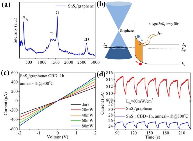
Wet chemical transfer techniques were used to deposit the highly transparent graphene film on the n-type SnS2 array film (as shown in Figure 1, to further improve the photoelectric performance of the device. The top-view SEM image of graphene/SnS2 heterostructure film is shown in Figure S3 (Supplementary Materials). The composition and microstructure of the samples were further analyzed by Raman (WITec Alpha 300R). As shown in Figure 5a, the intense peak at 315 cm−1 is assigned to the A1g mode of SnS2 array film. The presence of the peaks at 1352 cm−1, 1585 cm−1 and 2720 cm−1 corresponds to the D, G and 2D bands of graphene, respectively. The results show that the graphene/SnS2 composites were successfully fabricated. Figure 5c shows the I-V curves of a graphene/SnS2 heterostructure photodetector in the dark and at a light illumination intensity of 20 mW/cm2, 40 mW/cm2, 60 mW/cm2 and 80 mW/cm2, respectively. The asymmetry and nonlinearity of the curves indicates the non-ohmic contact between the graphene/SnS2 heterostructure [ref. 48,ref. 49]. As the light power density increases, the photocurrent intensity increases, indicating an effective photoresponse property. Figure 5d shows the I-t curves of the pure SnS2 array film and the graphene/SnS2 composites film under the same light illumination conditions. The graphene/SnS2 composites film has stable photoresponse characteristics and good reproducibility. The device based on graphene/SnS2 heterojunction has an increase in photocurrent of approximately 13.7 μA/cm2 compared with that of pure SnS2-based photodetectors. The on-off currents ratio (Ion/Ioff) of graphene/SnS2 heterojunction is 1.53, higher than that of pure SnS2 film with 1.1. The results show that the high off current and low on-off current ratio may be due to the low contact resistance between graphene and SnS2 layers; further improvement could be made by modifying the device configuration in the future. Furthermore, the response time (rise time/decay time) of the hybrid graphene/SnS2 film is 5 s/4.9 s, which is superior to that of the pure SnS2 array film (5.4 s/5.1 s). Under a high power light illumination, due to the abundance of photogenerated electron-hole pairs, the photogenerated carriers pass through the electrode for a long time, the current slowly rises to the optimal value, and the response time is long. The enhanced photoelectric performance is because graphene as a hole transporting layer was introduced by a simple transfer method to form a Schottky junction photodetector with vertical SnS2 array film. As already known, graphene has a zero-band gap characteristic resulting from its valence bands exhibiting linear dispersion degeneration near Dirac point energy. Nevertheless, under a built-in electric field formed at the interface between graphene and SnS2 array film, graphene can be tuned to display p-type behavior, as shown in Figure 5b [ref. 50]. Once incident photons are absorbed by SnS2 nanosheets array film, electron–hole pairs are predominantly produced in the depletion layer. The photo-generated holes transfer swiftly to the graphene and are collected by Au electrodes. The Schottky junction is beneficial for effective charge carrier separation. Consequently, the recombination of the photogenerated electrons and holes are effectively inhibited, leading to improved photoresponse performance. Moreover, since the graphene/SnS2 interface has charge trap states in ambient conditions, it reduces the dark current. We repeated the measurement in the vacuum environment (INSTEC, LTS420E-PB4, CO, USA), and the current was measured by Keithley 2636B (Tektronix, OH, USA). The results are shown in Figure S4 (Supplementary Materials), which shows that the dark current in the vacuum is lower than that in the ambient, thus the photoelectric response is improved. In addition, there are many methods [ref. 51] to improve the performance of photodetectors based on 2D materials, including surface plasma enhancement, charge transfer assistance, optical waveguide integration, graphene sandwich structure and heterogeneous structure directly grown by CVD. A high concentration of defects can reduce the mobility of carriers, [ref. 52] which is an important reason for the slow response of photodetectors. Further research will focus on reducing defects in the sample and improving device fabrication processes.
4. Conclusions
In summary, 2D SnS2/graphene composites film has been fabricated in situ on FTO by using low-temperature CBD and then the direct wet-chemical transfer method. The hybrid graphene/SnS2 film exhibits superior photoelectric performance compared to pristine SnS2 nanosheets array film. The light on/off ratio for SnS2 nanosheets is 1.1, whereas for the graphene/SnS2 composite, it is 1.53. The successful demonstration of the photoelectric enhancement based on 2D graphene/SnS2 array film opens up new opportunities for the application of other low-temperature soluble transition metal sulfide combined with graphene in photodetectors.
References
- K.S. Novoselov, V.I. Fal’Ko, L. Colombo, P.R. Gellert, M.G. Schwab, K. Kim. A roadmap for graphene. Nature, 2012. [DOI | PubMed]
- F. Xia, T. Mueller, Y.M. Lin, A. Valdes-Garcia, P. Avouris. Ultrafast graphene photodetector. Nat. Nanotechnol., 2009. [DOI | PubMed]
- J.V. Anguita, M. Ahmad, S. Haq, J. Allam, S.R.P. Silva. Nanotechnology: Ultra-broadband light trapping using nanotextured decoupled graphene multilayers. Sci. Adv., 2016. [DOI | PubMed]
- J. Ma, H. Huang, K. Ning, X. Xu, G. Xie, L. Qian, K.P. Loh, D. Tang. Generation of 30 fs pulses from a diode-pumped graphene mode-locked Yb:CaYAlO4 laser. Opt. Lett., 2016. [DOI | PubMed]
- L. Liu, H. Yao, H. Li, Z. Wang, Y. Shi. Recent advances of low-dimensional materials in lasing applications. FlatChem, 2018. [DOI]
- B. Liu, Y. Chen, C. You, Y. Liu, X. Kong, J. Li, S. Li, W. Deng, Y. Li, H. Yan. High performance photodetector based on graphene/MoS2/graphene lateral heterostrurcture with Schottky junctions. J. Alloys Compd., 2019. [DOI]
- S. Cakmakyapan, P.K. Lu, A. Navabi, M. Jarrahi. Gold-patched graphene nano-stripes for high-responsivity and ultrafast photodetection from the visible to infrared regime. Light Sci. Appl., 2018. [DOI | PubMed]
- C. Xie, C. Mak, X. Tao, F. Yan. Photodetectors Based on Two-Dimensional Layered Materials Beyond Graphene. Adv. Funct. Mater., 2017. [DOI]
- J. Zhang, L. Huang, Y. Zhang, Y. Xue, E. Zhang, H. Wang, Z. Kong, J. Xi, Z. Ji. Controlled synthesis of graphene nanoribbons for field effect transistors. J. Alloys Compd., 2015. [DOI]
- Y. Shi, W. Fang, K. Zhang, W. Zhang, L.J. Li. Photoelectrical response in single-layer graphene transistors. Small, 2009. [DOI | PubMed]
- M.F. El-Kady, Y. Shao, R.B. Kaner. Graphene for batteries, supercapacitors and beyond. Nat. Rev. Mater., 2016. [DOI]
- Z. Liu, S.P. Lau, F. Yan. Functionalized graphene and other two-dimensional materials for photovoltaic devices: Device design and processing. Chem. Soc. Rev., 2015. [DOI | PubMed]
- L.K. Putri, W.J. Ong, W.S. Chang, S.P. Chai. Heteroatom doped graphene in photocatalysis: A review. Appl. Surf. Sci., 2015. [DOI]
- X. Li, J. Yu, S. Wageh, A.A. Al-Ghamdi, J. Xie. Graphene in Photocatalysis: A Review. Small, 2016. [DOI | PubMed]
- M. Li, C.H. Chen, Y. Shi, L.J. Li. Heterostructures based on two-dimensional layered materials and their potential applications. Mater. Today, 2016. [DOI]
- W. Ouyang, F. Teng, J.H. He, X. Fang. Enhancing the Photoelectric Performance of Photodetectors Based on Metal Oxide Semiconductors by Charge-Carrier Engineering. Adv. Funct. Mater., 2019. [DOI]
- S.L. Danilishin, E. Knyazev, N.V. Voronchev, F.Y. Khalili, C. Gräf, S. Steinlechner, J.S. Hennig, S. Hild. A new quantum speed-meter interferometer: Measuring speed to search for intermediate mass black holes article. Light Sci. Appl., 2018. [DOI | PubMed]
- X. Liu, L. Gu, Q. Zhang, J. Wu, Y. Long, Z. Fan. All-printable band-edge modulated ZnO nanowire photodetectors with ultra-high detectivity. Nat. Commun., 2014. [DOI | PubMed]
- T. Mueller, F. Xia, P. Avouris. Graphene photodetectors for high-speed optical communications. Nat. Photonics, 2010. [DOI]
- J. Zhang, M.A. Itzler, H. Zbinden, J.W. Pan. Advances in InGaAs/InP single-photon detector systems for quantum communication. Light Sci. Appl., 2015. [DOI]
- R.R. Nair, P. Blake, A.N. Grigorenko, K.S. Novoselov, T.J. Booth, T. Stauber, N.M.R. Peres, A.K. Geim. Fine structure constant defines visual transparency of graphene. Science, 2018. [DOI]
- X. Chen, Z. Huang, X. Ren, G. Xu, J. Zhou, Y. Tao. Photodetectors Based on SnS2/Graphene Heterostructure on Rigid and Flexible Substrates. ChemNanoMat, 2018. [DOI]
- H. Li, Y. Shi, L.J. Li. Synthesis and optoelectronic applications of graphene/transition metal dichalcogenides flat-pack assembly. Carbon N. Y., 2018. [DOI]
- X.Y. Zhang, S.H. Sun, X.J. Sun, Y.R. Zhao, L. Chen, Y. Yang, W. Lü, D.B. Li. Plasma-induced, nitrogen-doped graphene-based aerogels for high-performance supercapacitors. Light Sci. Appl., 2016. [DOI | PubMed]
- Y. Du, Z. Yin, X. Rui, Z. Zeng, X.J. Wu, J. Liu, Y. Zhu, J. Zhu, X. Huang, Q. Yan. A facile, relative green, and inexpensive synthetic approach toward large-scale production of SnS2 nanoplates for high-performance lithium-ion batteries. Nanoscale, 2013. [DOI | PubMed]
- Y. Zhao, X. Li, B. Yan, D. Li, S. Lawes, X. Sun. Significant impact of 2D graphene nanosheets on large volume change tin-based anodes in lithium-ion batteries: A review. J. Power Sources, 2015. [DOI]
- M.S. Balogun, W. Qiu, J. Jian, Y. Huang, Y. Luo, H. Yang, C. Liang, X. Lu, Y. Tong. Vanadium Nitride Nanowire Supported SnS2 Nanosheets with High Reversible Capacity as Anode Material for Lithium Ion Batteries. ACS Appl. Mater. Interfaces, 2015. [DOI | PubMed]
- M. Haghighi, M. Minbashi, N. Taghavinia, D.H. Kim, S.M. Mahdavi, A.A. Kordbacheh. A modeling study on utilizing SnS2 as the buffer layer of CZT(S, Se) solar cells. Sol. Energy, 2018. [DOI]
- E. Zhao, L. Gao, S. Yang, L. Wang, J. Cao, T. Ma. In situ fabrication of 2D SnS2 nanosheets as a new electron transport layer for perovskite solar cells. Nano Res., 2018. [DOI]
- T. Di, B. Zhu, B. Cheng, J. Yu, J. Xu. A direct Z-scheme g-C3N4/SnS2 photocatalyst with superior visible-light CO2 reduction performance. J. Catal., 2017. [DOI]
- L. Dashairya, M. Sharma, S. Basu, P. Saha. SnS2/RGO based nanocomposite for efficient photocatalytic degradation of toxic industrial dyes under visible-light irradiation. J. Alloys Compd., 2019. [DOI]
- L. Jianzhe, X. Congxin, L. Honglai, P. Anlian. High on/off ratio photosensitive field effect transistors based on few layer SnS2. Nanotechnology, 2016
- X. Zhou, Q. Zhang, L. Gan, H. Li, T. Zhai. Large-Size Growth of Ultrathin SnS2 Nanosheets and High Performance for Phototransistors. Adv. Funct. Mater., 2016. [DOI]
- X. Jia, C. Tang, R. Pan, Y. Long, C. Gu, J. Li. Thickness-Dependently Enhanced Photodetection Performance of Vertically Grown SnS2 Nanoflakes with Large Size and High Production. ACS Appl. Mater. Interfaces, 2018. [DOI | PubMed]
- L. Gao, C. Chen, K. Zeng, C. Ge, D. Yang, H. Song, J. Tang. Broadband, sensitive and spectrally distinctive SnS2 nanosheet/PbS colloidal quantum dot hybrid photodetector. Light Sci. Appl., 2016. [DOI | PubMed]
- C. Fan, Y. Li, F. Lu, H.X. Deng, Z. Wei, J. Li. Wavelength dependent UV-Vis photodetectors from SnS2 flakes. RSC Adv., 2015. [DOI]
- G. Su, V.G. Hadjiev, P.E. Loya, J. Zhang, S. Lei, S. Maharjan, P. Dong, P.M. Ajayan, J. Lou, H. Peng. Chemical vapor deposition of thin crystals of layered semiconductor SnS2 for fast photodetection application. Nano Lett., 2015. [DOI | PubMed]
- Y. Tao, X. Wu, W. Wang, J. Wang. Flexible photodetector from ultraviolet to near infrared based on a SnS2 nanosheet microsphere film. J. Mater. Chem. C, 2015. [DOI]
- S. Gedi, V.R.M. Reddy, B. Pejjai, C. Park, C.W. Jeon, T.R.R. Kotte. Studies on chemical bath deposited SnS2 films for Cd-free thin film solar cells. Ceram. Int., 2017. [DOI]
- G. Ham, S. Shin, J. Park, J. Lee, H. Choi, S. Lee, H. Jeon. Engineering the crystallinity of tin disulfide deposited at low temperatures. RSC Adv., 2016. [DOI]
- A. Voznyi, V. Kosyak, L. Grase, J. Vecstaudža, P. Onufrijevs, Y. Yeromenko, A. Medvid, A. Opanasyuk. Formation of SnS phase obtained by thermal vacuum annealing of SnS2 thin films and its application in solar cells. Mater. Sci. Semicond. Process., 2018. [DOI]
- J. Kang, D. Shin, B. Hee. Graphene transfer: Key for applications. Nanoscale, 2012. [DOI | PubMed]
- N. Gao, X. Fang. Synthesis and Development of Graphene–Inorganic Semiconductor Nanocomposites. Chem. Rev., 2015. [DOI | PubMed]
- Y. Shi, K.K. Kim, A. Reina, M. Hofmann, L. Li, J. Kong. Work Function Engineering of Graphene Electrode via Chemical Doping. ACS Nano, 2010. [DOI | PubMed]
- P.U. Bhaskar, G.S. Babu, Y.B.K. Kumar, Y. Jayasree, V.S. Raja. Effect of bath concentration, temperature on the growth and properties of chemical bath deposited ZnS films. Mater. Chem. Phys., 2012. [DOI]
- A.S. Kavasoglu, F. Yakuphanoglu, N. Kavasoglu, O. Pakma, O. Birgi, S. Oktik. The analysis of the charge transport mechanism of n-Si/MEH-PPV device structure using forward bias I–V–T characteristics. J. Alloys Compd., 2010. [DOI]
- P. Gu, X. Zhu, H. Wu, J. Li, D. Yang. Influence of oxygen vacancy on the response properties of TiO2 ultraviolet detectors. J. Alloys Compd., 2019. [DOI]
- H.J. Hwang, E. Chang, B. Yoo, H. Shim. A graphene barristor using nitrogen profile controlled ZnO Schottky contacts. Nanoscale, 2017. [DOI | PubMed]
- J. Sheng, K. Fan, D. Wang, C. Han, J. Fang, P. Gao, J. Ye. Improvement of the SiOx Passivation Layer for High-Efficiency Si/PEDOT: PSS Heterojunction Solar Cells. ACS Appl. Mater. Interfaces, 2014. [DOI | PubMed]
- C.E.E. Rao, A.E. Sood, K.E. Subrahmanyam, A. Govindaraj. Graphene: The new two-dimensional nanomaterial. Angew. Chem. Int. Ed., 2009. [DOI]
- F. Yan, Z. Wei, X. Wei, Q. Lv, W. Zhu, K. Wang. Toward High-Performance Photodetectors Based on 2D Materials: Strategy on Methods. Small Methods, 2018. [DOI]
- J. Lu, C. Xu, J. Dai, J. Li, Y. Wang, Y. Lin, P. Li. Improved UV photoresponse of ZnO nanorod arrays by resonant coupling with surface plasmons of Al nanoparticles. Nanoscale, 2015. [DOI | PubMed]