Low-cost fabrication methods of ZnO nanorods and their physical and photoelectrochemical properties for optoelectronic applications
Abstract
Zinc Oxide (ZnO) nanorods have great potential in several applications including gas sensors, light-emitting diodes, and solar cells because of their unique properties. Here, three low cost and ecofriendly techniques were used to produce ZnO nanorods on FTO substrates: hydrothermal, chemical bath deposition (CBD), and electrochemical deposition (ECD). This study explores the impact of such methods on the optical, structural, electrical, morphological, and photoelectrochemical properties of nanorods using various measurements. XRD analysis confirmed the hexagonal wurtzite structure of ZnO nanorods in all three methods, with hydrothermal showing a preferred orientation (002) and CBD and ECD samples showing multiple growth directions, with average particle sizes of 31 nm, 34 nm, and 33 nm, respectively. Raman spectra revealed hexagonal Wurtzite structure of ZnO, with hydrothermal method exhibiting higher E2 (high) peak at 438 cm−1 than CBD and ECD methods. SEM results revealed hexagonal ZnO nanorods became more regular and thicker for the hydrothermal method, while CBD and ECD led to less uniform with voids. UV-vis spectra showed absorption lines between 390 nm and 360 nm. Optical bandgap energies were calculated as 3.32 eV, 3.22 eV, and 3.23 eV for hydrothermal, CBD, and ECD samples, respectively. PL spectra revealed UV emission band with a small intensity peak around 389 nm and visible emission peaks at 580 nm. Temperature dependent PL measurements for ZnO nanorods indicated that the intensities ratio between bound exciton and free exciton decreases with temperature increases for the three methods. Photocurrent measurements revealed ZnO nanorod films as n-type semiconductors, with photocurrent values of 2.25 µA, 0.28 µA, and 0.3 µA for hydrothermal, CBD, and ECD samples, and photosensitivity values of 8.01, 2.79, and 3.56 respectively. Our results suggest that the hydrothermal method is the most effective approach for fabricating high-quality ZnO nanorods for optoelectronic applications.
Article type: Research Article
Keywords: Low-cost, Hydrothermal, Chemical bath deposition, Electrochemical deposition, ZnO nanorods, Physical and photoelectrochemical properties, Optoelectronic applications, Engineering, Materials science, Optics and photonics, Physics
Affiliations: https://ror.org/04a97mm30grid.411978.20000 0004 0578 3577Physics Department, Faculty of Science, Kafrelsheikh University, Kafrelsheikh, 33516 Egypt; https://ror.org/04a97mm30grid.411978.20000 0004 0578 3577NanoScience and Technology Program, Faculty of Science, Kafrelsheikh University, Kafrelsheikh, 33516 Egypt
License: © The Author(s) 2024 CC BY 4.0 Open Access This article is licensed under a Creative Commons Attribution 4.0 International License, which permits use, sharing, adaptation, distribution and reproduction in any medium or format, as long as you give appropriate credit to the original author(s) and the source, provide a link to the Creative Commons licence, and indicate if changes were made. The images or other third party material in this article are included in the article’s Creative Commons licence, unless indicated otherwise in a credit line to the material. If material is not included in the article’s Creative Commons licence and your intended use is not permitted by statutory regulation or exceeds the permitted use, you will need to obtain permission directly from the copyright holder. To view a copy of this licence, visit http://creativecommons.org/licenses/by/4.0/.
Article links: DOI: 10.1038/s41598-024-73352-5 | PubMed: 39394341 | PMC: PMC11470147
Relevance: Relevant: mentioned in keywords or abstract
Full text: PDF (2.8 MB)
Introduction
ZnO nanorods have garnered a lot of interest lately due to their unique characteristics and wide range in many applications1. In nanotechnology, one-dimensional nanostructures are remarked for their remarkable electrical, optical, and mechanical properties making them ideal for various technological innovations2. ZnO nanorods’ huge surface area, wide band gap, strong exciton binding energy, and high aspect ratio make them very advantageous for usage in solar cells3, light-emitting diodes4, photodetectors5, photocatalysts6, and biosensors7. ZnO is a non-toxic, chemically stable, and accessible material abundant in the earth8–10. ZnO is an extrinsic semiconductor known as an n-type semiconductor with a bandgap of almost 3.37 eV and has high exciton-binding energy (60 meV)10–13. Recently, the preparation of ZnO nanostructures as nanowires, nanorods, nanotubes, and nanoflowers has gained growing attention8,14–16. Physical techniques like molecular beam epitaxy17, metal-organic chemical vapor deposition18, sputtering19, and pulsed laser deposition20 can be used to produce ZnO. However, such methods are expensive due to the requirement for high temperatures and low pressures, and equipment complexity. On the other hand, simplifying their manufacturing processes leads to high technical developments for industrial applications. So chemical methods such as hydrothermal deposition21, chemical bath deposition22, and electrochemical deposition13 are cost-effective, large-scale production potential and highly efficient for manufacturing nanoparticles for various applications.
Asmaa Al-Rasheedi et al. studied salt concentration on ZnO nanorods using hydrothermal methods. They found that higher salt concentrations increased rod diameter and crystallite size but reduced length, as confirmed by XRD analysis21. Min Wang and colleagues synthesized Cu-Ni co-doped ZnO nanorods on FTO substrates via a hydrothermal method. The co-doped nanorods were grown with added nickel and copper nitrates, enhanced photocatalytic degradation by generating electron-hole pairs under UV light, leading to increased free-carrier concentration and improved azo dye degradation23. (A) Kathalingam et al. used a unique chemical solution approach to synthesis ZnO nanostructures using different precursors and investigated the effects of bath concentration and temperature on ZnO nanostructures. By varying the HMT content, rod size and shape might be altered. Seamless long nanorods with a sheet-like shape were created using the zinc acetate and NaOH method. By manipulating the size and shape of the nanorods, the work was able to fabricate two terminal planar nanorod devices with distinct I-V nature24. L.V. Podrezova and colleagues used the hydrothermal method to grow ZnO nanorods on various conductive substrates, including metals like Cu, Ni, Pt, Ag, Au, and FTO. They prepared a ZnO seed layer using sol-gel spin coating and a growth solution containing zinc nitrate hexahydrate, hexamethylenetetramine, polyethylenimine, and ammonium hydroxide. The synthesis was carried out at 88 °C for 2 h. The resulting ZnO nanorods were vertically aligned, with the most ordered arrays observed on Au substrates25. Pooja (B) More et al. synthesized ZnO thin films on FTO substrates using a chemical bath deposition method. The films had a hexagonal wurtzite structure and rod structures with an average height of 630 nm and width of 340 nm. The optical band gap was 3.1 eV, and electrochemical tests confirmed n-type conductivity with a charge carrier density of 8.55 × 1018 cm−322. Büşra Altun and colleagues studied the effects of cobalt doping on ZnO thin film sensors, focusing on their structural, optical, and CO2 gas sensing properties. They doped ZnO with 1%, 3%, 5%, and 7% cadmium using chemical bath deposition. The 3% Cd-doped sensor had the highest CO2 response, fast response times, good selectivity, and high stability26. Sanghyeon Moon and colleagues created ZnO nanorods on FTO glasses and ZnO nanoparticle-coated FTO glasses using chemical bath deposition. SEM images showed nanorod widths of 500 nm on FTO and 100 nm on nanoparticle-coated FTO. Electrochemical impedance spectroscopy (EIS) revealed lower charge transfer resistance and faster reaction kinetics for ZnO nanorods on FTO glasses27. Dubey and Saravanam studied the impact of negative potentials (-0.5 to -1.5 V) on ZnO nanostructures grown on FTO substrates for dye-sensitized solar cells. They used a zinc chloride and potassium chloride solution, three electrode configurations, and annealed samples at 400 °C for 1 h. UV-vis spectra showed increased absorption and redshift with higher potentials, while fluorescence spectra showed maximum emission at 650 nm at -1.5 V28. Sigamani Saravanan and colleagues created ZnO nanostructures on a thin film coated FTO substrate using spin coating and electrochemical techniques. They prepared a transparent Zn-doped TiO2 solution and aged it for 24 h before depositing it on the FTO substrate. The samples were heated in a muffle furnace and then electrochemically deposited using a three-electrode setup. The samples were calcined again and characterized using XRD peaks for anatase TiO2 and ZnO’s hexagonal wurtzite structure. Raman spectroscopy revealed ZnO phonon modes at 444 cm−129. Daniel Solís-Cortés and his team studied the growth of ZnO nanorods on different transparent conductive oxide (TCO) substrates, including FTO, ITO, and IZO. They used linear sweep voltammetry in a three-electrode electrochemical cell, maintaining a 70 °C electrolyte solution and deposition at -0.700 V vs. SCE for 3600 s. The results showed that ZnO density was highest on IZO (7.83 × 10⁸ cm⁻²), with nanorod diameters ranging from 225 to 259 nm. XRD and HRTEM confirmed that IZO supports denser and better-aligned ZnO nanorods due to its optimal nucleation sites and improved vertical alignment30.
In this work, three chemical processes; hydrothermal deposition, chemical bath deposition, and electrochemical deposition will be utilized to produce ZnO nanorods on FTO substrates and explore the impact of such method on the optical, structural, electrical, morphological, and photoelectrochemical properties of nanorods using various measurements. X-ray diffraction (XRD), Raman spectroscopy, scanning electron microscopy (SEM), UV-vis spectroscopy, photocurrent measurements, and photoluminescence spectroscopy (PL) at room temperature and different temperatures.
Experimental methods
Synthesis of ZnO NRs
Prior to manufacturing ZnO nanorods using three different methods; hydrothermal, chemical bath deposition, and electrochemical deposition, fluorine-doped tin oxide (FTO) substrates underwent a standard cleaning procedure. This involved a 10-minute ultrasonic bath with acetone, isopropanol, and deionized water (Milli-Q, 18 MΩ.cm at 25 °C), respectively. Then, the substrates were dried for 4 h at 100 °C.
Grow of ZnO nanorods by hydrothermal method
The hydrothermal method was chosen for growing ZnO nanorods on FTO substrates due to its precise control over growth conditions, low substrate protection, uniform, aligned, and crystalline nanorods, and its environmental friendliness and cost-effectiveness for large-scale production.
ZnO nanorods were synthesized on a 2 cm × 2 cm FTO substrate by a hydrothermal process without seed layers13,31. The Zn2+ ions source was prepared as a 40 mL solution of 2,975 g of 0.25 M zinc nitrate hexahydrate [Zn(NO3)2·6H2O, Sigma-Aldrich, 99%] with a 40 mL solution of 4.71 g of 2.1 M potassium hydroxide [KOH, Sigma-Aldrich, 99.5%]. The solution was mixed together for 10 min. and then transferred to a Teflon-lined autoclave where FTO substrates were placed vertically. The autoclave was then maintained at 150 °C for 16 h. Afterward, the grown samples were rinsed several times with distilled water and allowed to air-dry for additional characterization32.
Grow of ZnO nanorods by chemical bath deposition (CBD) method
The chemical bath deposition (CBD) method was chosen for fabricating ZnO nanorods on FTO substrates due to its simplicity, cost-effectiveness, and large-scale production accessibility. CBD operates at low temperatures and requires minimal equipment, allowing precise growth parameter control and nanorod property customization.
ZnO nanorods were created utilizing the procedure previously outlined in Sect. 2.1, but instead of using an autoclave, chemical bath deposition was employed33,34. In such method, the solution was transferred to a flask within a water bath at 80 °C for 4 h where substrates were vertically positioned35.
Grow of ZnO nanorods by electrochemical deposition method
The electrochemical deposition method was chosen for fabricating ZnO nanorods on FTO substrates due to its precise control over growth, customizable nanorod properties, adjustable size, density, and orientation, scalability, cost-effectiveness, and compatibility with various substrates due to its low-temperature operation.
ZnO nanorods were formed by electrochemical deposition where a three-electrode cell system was utilized in the experiment with the FTO substrate serving as the working electrode, Ag/AgCl as the reference electrode, and platinum wire as the counter electrode. The electrochemical deposition was carried out in a solution containing 0.017 g of 0.5 mM zinc chloride [ZnCl2, Sigma-Aldrich, 98%] and 1.86 g of 0.1 M potassium chloride [KCL, Sigma-Aldrich, 99%] with an applied voltage of − 0.7 V vs. Ag/AgCl electrode for one hour at 60 °C while stirring at 250 rpm3,36,37.
Based on the following processes at static-potential (E = -0.7 V/SCE), metal oxide is formed by a chemical reaction between the native hydroxides (OH-) and the metal cations in the solution38:
\begin{aligned}{O}_{2}+4e+2{H}_{2}O&\to 4O{H}^{-} \\ {Zn}^{2+}+2O{H}^{-}&\to ZnO+{H}_{2}O\end{aligned}
\]
To summarize, this is
{Zn}^{2+}+\frac{1}{2}{O}_{2}+2e\to ZnO
\]
Characterization techniques
X-ray diffraction (XRD, Shimadzu 6000) with 0.154 nm wavelength CuKα radiation. The XRD measurements were performed at a scan speed of 8.0°/min, a scan step of 0.02°, 40 kV, and 30 mA. And Raman spectroscopy (WITec alpha300 R setup with two laser sources; 532 nm, Max. 30 mW and 785 nm, Max. 133 mW) were used to investigate the crystal structures of our samples. A UV-Vis spectrophotometer (JASSCO V-630) was used to analyze the optical absorption spectra of the samples. A scanning electron microscope (JSM-651OLV) was employed to examine the samples’ morphology. The PL spectrophotometer (He-Cd laser, 325 nm, Max. 200 mW, and a Synapse CCD camera that was built into the HORIBA iHR320 spectrometer was used to record the spectra) was utilized to obtain valuable data on the samples’ quality and purity. The photocurrent was measured using a homemade setup that included a 200 W tungsten lamp for lighting, an illumination switch, a three-electrode cell with the FTO substrate serving as the working electrode, Ag/AgCl as the reference electrode, and platinum wire as the counter electrode, and a controlling Bio-logic system. Photocurrent measurements were performed at 0 Volts vis Ag/AgCl electrode in 0.5 M Na2SO4 solution that acted as the supporting electrolyte.
Results and discussions
XRD analysis
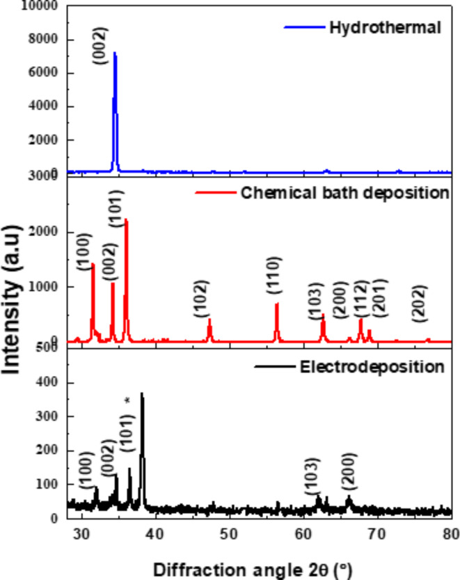
XRD patterns of ZnO nanorods with the different methods (hydrothermal, CBD, and electrodeposition) are shown in Fig. 1. The diffraction patterns are very comparable to the hexagonal wurtzite structure of ZnO (standard JCPDS Card No 65-3411) with lattice constant (a = 0.325 nm, c = 0.521 nm)39–42. In the case of chemical bath deposition and electrodeposition methods, ZnO nanorods existed in (100), (002), (101), (103), and (200) direction planes meaning that ZnO nanorods are shaped on FTO substrates in various orientations. The FTO crystallographic planes are correlated with (JCPDS No.77–0452)43.
By the following equations, the lattice constants (a and c) of ZnO nanorods were obtained44,45:
\frac{1}{{d}^{2}}=\frac{4}{3}\left(\frac{{h}^{2}+hk+{k}^{2} }{{a}^{2}}\right)+\frac{{l}^{2}}{{c}^{2}}
\]
when \(k=l=0\), lattice parameter a was found from
a=\frac{\lambda }{\sqrt{3} \text{sin}\theta } \sqrt{{h}^{2}+hk+{k}^{2}}
\]
when \(h=k=0\), lattice parameter c was found from
c=\frac{\lambda }{2 \text{sin}\theta } l
\]
where “d” is lattice spacing, \(\lambda\) the wavelength of CuKα radiation, \(\theta\) the Bragg diffraction angle in degree. It is found that (a = 0.3257 nm, c = 0.5226 nm) and (a = 0.333 nm, c = 0.516 nm) for chemical bath deposition and electrochemical deposition, respectively. For hydrothermal method, a high intensity preferred orientation (002) is noticed indicating the formation of ZnO nanorods perpendicular to FTO substrates in the c-axis direction with lattice constant c = 0.519 nm) due to high temperature promotes the creation of well-aligned nanorods by speeding up ZnO nucleation and development along this axis46. This can have an impact on the characteristics of ZnO by improving electron-hole pair radiative recombination, which can result in increased and more intense light emission, increased electron mobility, decreased recombination rates, and increased surface area.
The crystallite size has been calculated for ZnO nanorods by Scherer’s equation47:
D=\frac{K \lambda }{{\beta }_{hkl}\text{cos}\theta }
\]
where λ is the wavelength of CuKα radiation, θ is the Bragg diffraction angle in radians, D is the crystallite size in nanometers, K is the shape of factor (0⋅9), and \({\beta }_{hkl}\) is the peak width at half-maximal intensity in radians. The average crystallite sizes D are determined for hydrothermal, CBD, and ECD methods are calculated in Table 1.
Table 1: The optical band gaps\({E}_{g}\)photocurrent (µA), average diameter (nm), and average crystallite size D (nm) of ZnO nanorods produced by hydrothermal, chemical bath deposition, and electrochemical deposition methods.
| Method | \({\varvec{E}}_{\varvec{g}}\) (eV) | Photocurrent (µA) | Average Diameter (nm) | D (nm) |
|---|---|---|---|---|
| Hydrothermal | 3.32 | 2.26 | 180 | 31 |
| Chemical bath | 3.22 | 0.28 | 158 | 34 |
| Electrochemical | 3.23 | 0.30 | 146 | 33 |
The Zn-O bond length is obtained by equation48:
L= \sqrt{(\frac{{a}^{2}}{3}+{\left(\frac{1}{2}-u\right)}^{2}}*{c}^{2})
\]
In the wurtzite structure, u is the positional parameter that signifies the amount that each atom is moved along the ‘c’ axis with the subsequent one. It is provided by:
u= \frac{{a}^{2}}{3*{c}^{2} }+0.25
\]
The relationship between c/a and u indicates that when c/a declines, u increases in a way that keeps those four tetrahedral distances almost constant via a distortion of tetrahedral angles. The Zn-O bond length in the ZnO unit cell with surrounding atoms is 0.19767 nm48. The determined bond length of Zn-O is found to be 0.1983 nm and 0.2006 nm for chemical bath deposition and electrochemical deposition, respectively.
The determined bond length in the unit cell correlates with the Zn-O bond length. The results of XRD support the high purity of the ZnO nanorods synthesized and hence the strong crystalline nature because there are no impurity peaks.
Raman spectroscopy analysis
Researchers can better understand transport characteristics and phonon interactions with free carriers which impact device performance by using Raman measurements which reveal material quality, phase, and purity49. Therefore, we apply Raman spectroscopy to study the structure of ZnO nanorods. The Wurtzite-type ZnO has two formula units in the primitive cell50,51, and belongs to the space group C4 (P63mc), and single-crystalline ZnO exhibits eight sets of optical phonon modes at \(\Gamma\) point of the Brillouin zone, which are classified as52,53:
\Gamma_{opt}= 1{A}_{1}+2{B}_{I}+1{E}_{1}+2{E}_{2}.
\]
A1 + E1 + 2E2 modes (Raman active), 2B1 modes (Raman silent), and A1 + E1 modes (Raman silent) (infrared active). Both the A1 and E1 modes are polar and split into transverse optical (TO) and longitudinal optical (LO) phonons.
Raman spectra of ZnO NRs using three different methods at room temperature are shown in Fig. 2. Raman shifts are similar to those previously published53 which are attributed to ZnO nanorods. The main peaks at 100 and 438 cm−1 are Raman active and commonly observed in the wurtzite structure ZnO54 which are attributed to the low- and high- E2 modes of nonpolar optical phonons, respectively. A second-order nonpolar E2 mode55 which is Raman active only, and has been attributed to the weaker peak at 333 cm−1. The E2(high) for the hydrothermal method is clearly visible at 438 cm−1, and it is much higher than E2 (high) for CBD and electrochemical deposition methods, also full width at half maximum of this peak for hydrothermal method is narrow in comparison with CBD and ECD methods showing good crystal quality of self – assembling radial structures, and resulting in a more ordered crystal structure56. It is not immediately clear that the peak at 411 cm−1 relates to the E1(TO) mode. One of the distinctive features of the hexagonal wurtzite ZnO is the extremely powerful E2 (high) peak located at 438 cm−1. E1(TO) on the left-hand side of E2H is hidden by the asymmetrical and line-broadening properties. The E1(LO) mode is responsible for the peak at 578 cm−1 which is induced by defects such as oxygen vacancy, zinc interstitial, or their complexes and free carriers57. As ZnO contains a significant number of intrinsic defects. In particular, many surface defects in rod ZnO nanostructures will lead to a distribution of surface energy levels constituting the surface energy band. The excitation of surface states can be induced by sub-band gap excitation58. As a result, the visible Raman emission could be related to surface states. These defects can influence the efficiency of light emission and detection, and can impact the charge separation and collection efficiency in solar cells. Based on the relative intensity of E1(LO), we believe that electrochemical deposition has better crystal perfection than hydrothermal and CBD methods. In other words, the defect concentration in the hydrothermal method is somewhat larger than in CBD and electrochemical deposition methods.

Analysis of Surface morphology
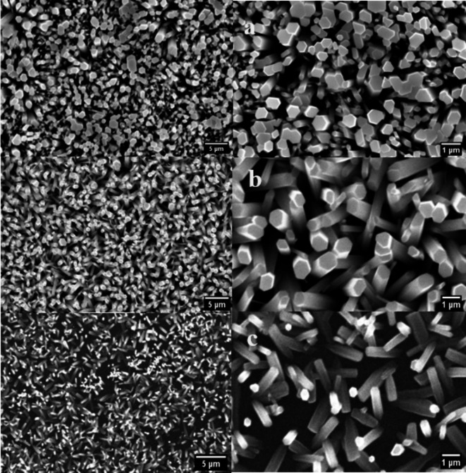
Figure 3 displays top-view SEM images of ZnO nanorods grown by hydrothermal, chemical bath deposition, and electrodeposition on FTO substrates. In the case of chemical bath deposition and electrodeposition methods, it is evident that ZnO was shaped in rod arrays with a hexagonal (wurtzite) structure and that the nanorods condensed to form nanorod shapes such as rod-like structures, not all the nanorods were perpendicular to the substrate where some voids appeared. This variation is due to the less controlled deposition environment and slower growth kinetics, which allow for more random growth directions and sizes [59, 60]. For hydrothermal method, the ZnO nanorods with hexagonal shapes become more regular and thicker where the voids vanished and nanorods cover the substrate’s surface with approximately one orientation along the c-axis on the FTO substrate [61]. This is because the hydrothermal conditions encourage the wurtzite structure’s development along its c-axis, producing well-ordered nanorods and a high aspect ratio. The average diameter of ZnO nanorods for three methods is calculated by using image J software as shown in table 1. The thickness and length of nanorods were calculated using the mass and density of samples before and after deposition and were found to be around 3, 2.5, and 1.5 μm. The XRD results have been confirmed by the SEM results where ZnO nanorods by chemical bath deposition and electrodeposition methods have a hexagonal structure with different orientation, while almost one c – axis orientation was observed for the hydrothermal method.
UV-Vis studies
V 630 spectrophotometer was used to investigate the optical characteristics of ZnO nanorods in a spectral range between 300 and 800 nm. Figure 4 displays UV- vis absorption spectra of ZnO nanorods where absorption peaks around 375 nm, 385 nm and 384 nm appeared for hydrothermal, chemical bath deposition, and electrochemical deposition, respectively. Such peaks are attributed to the movement of electrons between the valence band and the conduction band (O2p – Zn3d), which corresponds to the band gap and absorption peaks of ZnO62–64.
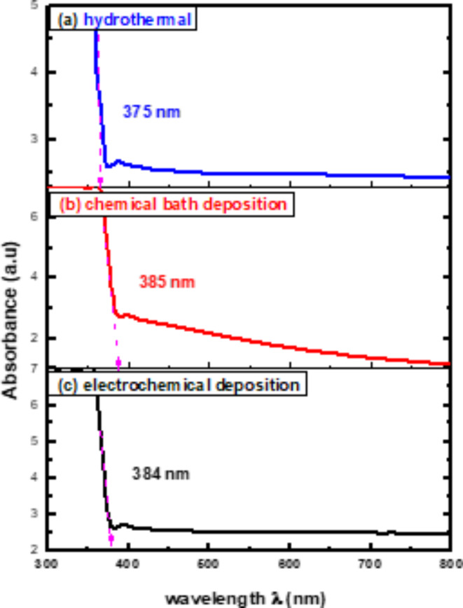
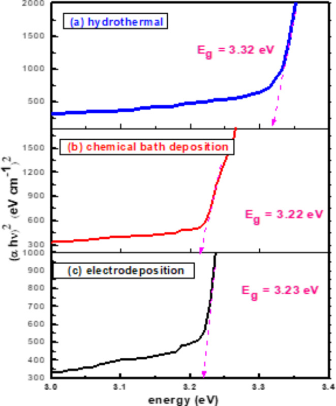
For direct band gap materials, the absorption coefficient could be calculated using The Tauc equation, \({\left(\alpha h\nu \right)}^{2}=K(h\nu – {E}_{g})\) at the absorbance edge. \({E}_{g}\) was estimated by extending the linear part of the dependency \({\left(\alpha h\nu \right)}^{2}\) on \(h\nu\) to the energy axis65–67. The calculated optical band gaps of ZnO nanorods are found in Table 1 for the hydrothermal method, chemical bath deposition method, and electrochemical deposition method, respectively as shown in Fig. 5.
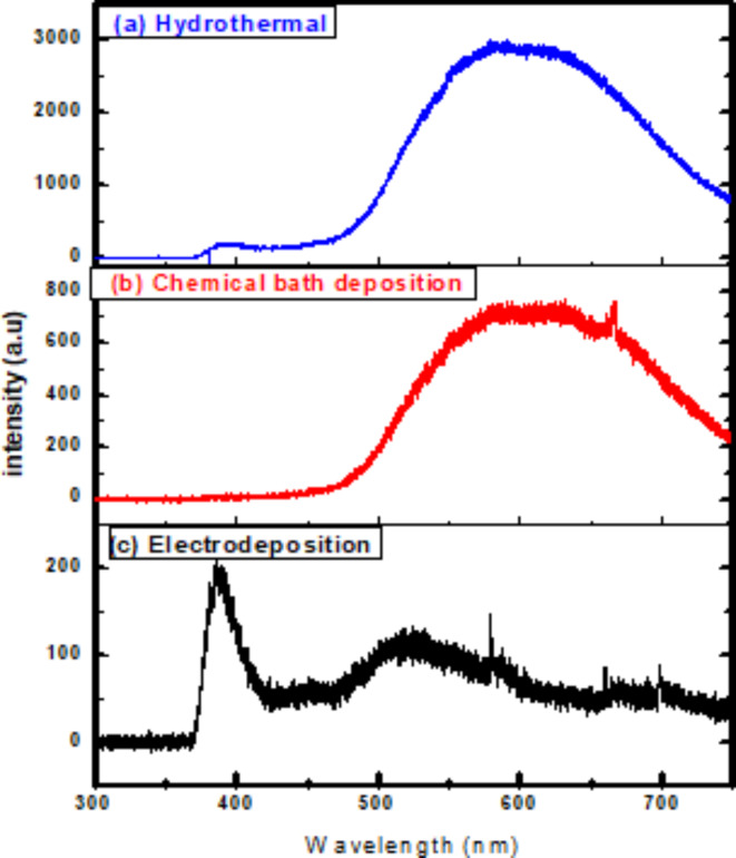
Photoluminescence (PL) analysis
PL is one of the most powerful semiconductor techniques for detecting the presence of defects where PL of ZnO nanorods was recorded at ambient temperature with excitation wavelength of 325 nm as shown in Fig. 6. Two emissions peaks are found in the spectrum of PL; UV and visible light ones with different relative strength of peaks and their location for different methods. UV emissions is referred to as Near Band Edge Emission of ZnO with a small peak at about 389 nm that could be resulted from the annihilation of the excitons as ZnO exhibits a high exciton binding energy at ambient temperature (60 meV)68–70. In the meantime, a broad emission peak in the visible range appeared due to the presence of deep level defects such as vacancies of single ionized oxygen and interstitial zinc or their complexes71,72. The large deep level emission and the weak UV band demonstrated the great potential of optoelectronic system applications for ZnO nanorods.
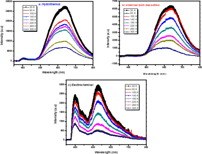
In order to learn more about the nature of point defects in ZnO nanorods, temperature-dependent PL spectra were studied in detail as shown in Fig. 7 where the measurements were performed between 20 and 300 K. It is evident that the intensity ratio of bound to free exciton falls with increasing temperature. This is because the bound exciton transition process outweighs when the thermal energy is less than the binding energy and the free exciton transition process supersedes when the thermal energy is greater. We can also see how defective emissions behave differently as a function of temperature. With increasing temperature, the green, red, and yellow emission peaks shift, and the intensity of the defect emission decreases in ZnO NRs by three methods. In the case of a high defect concentration, a broad and featureless emission is predicted due to the formation of an energy band rather than discrete defect levels73.
Photocurrent measurements
Photocurrent measurements were measured with a three-electrode electrochemical system with the FTO substrate serving as the working electrode, Ag/AgCl as the reference electrode, and platinum wire as the counter electrode. Where a broad-spectrum 200 W tungsten lamp illuminated the working electrode, manually switched on and off at predetermined intervals of time (30 s). The measurements were performed in 0.01 M sodium sulfate (Na2SO4). Bio-Logic Sb-50 potentiostat regulates both the applied voltage and scan rate at a bias potential of 0 V vs. Ag/AgCl where an electrochemical cell (PEC) was performed both in the dark and under light73.
The rise and decline of photocurrent in air under visible light is shown in Fig. 8 for all samples with a constant photo flux and zero bias voltage. The cell was maintained dark at first until the dark current was stable. In comparison, the current density in the dark is near to zero. However, in the presence of light, the curve exhibits an almost instantaneous and constant reaction, with a significant increase in current. The material is still being exposed to light as it scatters inside the nanorods. When the photogenerated current is positive, n-type conductivity is present74. This could be attributed to the formation of additional negative charges on the semiconductor’s surface when the samples were exposed to light. This light activation likely generated electrons, which then moved from the electrolyte to the grown film, leading to the emergence of upward photocurrents75,76. Even during illumination, the photocurrent began to gradually decline after reaching a high. The delayed process of photoinduced chemisorption of oxygen molecules on the surface of ZnO nanostructures could explain this strange phenomenon77. When the irradiation is turned off, the photocurrent quickly drops to nearly zero, and it returns to normal as soon as the light is switched back on. This indicates that the current is entirely driven by the photoelectrode’s response to visible light and that the charge transport is extremely rapid78–80.
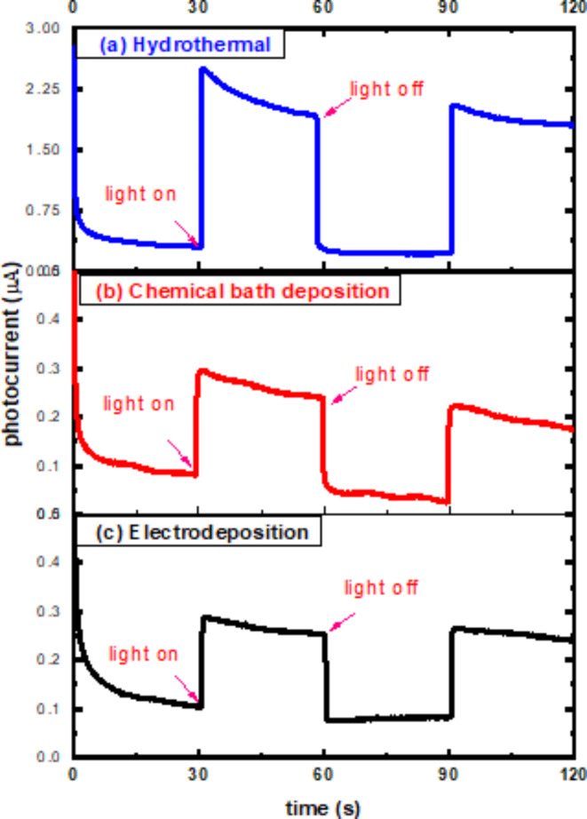
In photoconductivity measurements, the photosensitivity (η) is an important parameter which is defined as the maximal photocurrent (Ipc) divided by the dark current (Idc). The photosensitivity illustrates the dependence of the defect state density on temperature, composition, and light intensity in the gap. The computed values of η for each sample at room temperature are listed in Table 2.
Table 2: The rise and decay time constants \({\tau }_{r}\) (s), \({\tau }_{d}\) (s), trap ionization energies (trap depth, eV) of different traps corresponding to different exponentials and photosensitivity η for three methods.
| Method | \({\varvec{\tau }}_{\varvec{r}}\) (s) | \({\varvec{\tau }}_{\varvec{d}}\) (s) | Η | Trap depth (eV) |
|---|---|---|---|---|
| Hydrothermal | 0.2 | 0.239 | 8.01 | 0.496 |
| Chemical bath | 0.346 | 0.839 | 2.79 | 0.508 |
| Electrochemical | 0.243 | 1.29 | 3.56 | 0.522 |
The value of η is determined by the excess carrier lifetime which is determined by the density of localized states in each material. Because defect states operate as recombination centers in the presence of light, the larger the density of defect states, the shorter the lifetime. As a result, the photosensitivity changes could be related to a change in defect state density with composition81.
The trap depths may be determined by separating the decaying part of the current rise and decay time response curves into the potential number of exponentials. The exponentials are calculated using the Eqs82,83:
I= {I}_{0}\text{exp}(-pt)
\]
where \({I}_{0}\) represents the current when the light is turned off, I represents the photocurrent at any given time, and p is the probability of an electron escaping from the trap each second, which has a different value for each exponential section. The chance of an electron escaping from a trap can also be calculated using the following equation:
I= S\text{exp}(-E/KT)
\]
where K is the Boltzmann constant (1.381 \(\times\)10−23 J/K), T is the absolute temperature, and S is the frequency factor that gives the rate at which quanta from crystal vibrations (phonons) try to eject electrons from traps multiplied by the probability of transition from trap to the conduction band and it has a value of 109 at room temperature84–86.
Using the preceding equations, the trap depths (E) corresponding to various exponentials are determined and represented by:
E=KT\left[\text{ln}S-\text{ln}\frac{\text{ln}\left(\raisebox{1ex}{${I}_{0}$}\!\left/ \!\raisebox{-1ex}{$I$}\right.\right)}{t}\right]
\]
The trap depth is calculated from the decay portion of the curve shown in Fig. 8 for all methods and its values are presented in Table 2.
Conclusion
We have documented the development of vertically growing ZnO nanorods on FTO substrates using low cost and ecofriendly hydrothermal, chemical bath deposition and electrochemical processes. The structure, morphological, optical, and photoelectrochemical of the synthesized ZnO nanorods are investigated using XRD, Raman spectroscopy, SEM, UV-Vis, PL, and photocurrent measurements. XRD of ZnO films by hydrothermal method showed a high intensity preferred orientation (002), while chemical bath and electrochemical deposition methods shaped ZnO in various orientations. The Raman scattering spectra of ZnO NRs show that the hydrothermal method exhibited a higher E2 peak at 438 cm-1 where active in the wurtzite structure ZnO, indicating good crystal quality of self-assembling radial structures. SEM results showed that hexagonal ZnO nanorods became more regular and thicker with voids disappearing for hydrothermal methods. The UV-vis spectra showed absorption edges at 378 nm, 389 nm, and 366 nm, corresponding to electron transfer from the valence band to the conduction band of ZnO nanorods. PL results showed that ZnO nanorods emit UV and visible light peaks which produce exciton annihilation and deep defects. The temperature-dependent PL measurements indicated decreasing in intensity ratio between bound and free excitons. Photocurrent measurements showed n-type conductivity for all the fabricated samples where the hydrothermal method had more carriers due to increased current intensity. Our results indicate that the fabricated ZnO nanorods with the hydrothermal method is the preferred for optoelectronic applications.
References
- PK Aspoukeh, AA Barzinjy. Synthesis, properties and uses of ZnO nanorods: A mini review. Int. Nano Lett., 2022. [DOI]
- 2.Tang, Z., Zhang, J., Y.J.A.F, M. & Zhang. Renaissance of one-dimensional nanomaterials. Adv. Funct. Mater.32(11) (2022).
- F Qiao. Design strategies of ZnO heterojunction arrays towards effective photovoltaic applications. Battery Energy, 2022. [DOI]
- MA Rahman. ZnO nanorods on Li-doped ZnO thin films for efficient p–n homojunction light-emitting diodes. ACS Appl. Nano Mater., 2023. [DOI]
- L Chu. Fabrication and application of different nanostructured ZnO in ultraviolet photodetectors: A review. IEEE Sens. J., 2022. [DOI]
- PG Ramos. A review on improving the efficiency of photocatalytic water decontamination using ZnO nanorods. J. Solgel Sci. Technol., 2022. [DOI]
- M Saeed. Recent advances, challenges, and future perspectives of ZnO nanostructure materials towards energy applications. Chem. Rec., 2024. [DOI | PubMed]
- S Raha, MJNA Ahmaruzzaman. ZnO nanostructured materials and their potential applications: Progress, challenges and perspectives. Nanoscale Adv., 2022. [DOI | PubMed]
- MJCI Hessien. Recent progress in zinc oxide nanomaterials and nanocomposites: From synthesis to applications. Ceram. Int., 2022. [DOI]
- 10.Rai, H. & Kondal, N. J. M. T. P. A review on defect related emissions in undoped ZnO nanostructures. Mater. Today Proc.48, 1320–1324 (2022).
- I Ayoub. Advances in ZnO: Manipulation of defects for enhancing their technological potentials. Nanatechnol. Rev, 2022. [DOI]
- R Rasmidi. Radiation damage effects on zinc oxide (ZnO) based semiconductor devices–a review. Radiat. Phys. Chem., 2021. [DOI]
- CV Manzano. Recent progress in the electrochemical deposition of ZnO nanowires: Synthesis approaches and applications. Crit. Rev. Solid State Mater. Sci., 2022. [DOI]
- MS Krishna. A review on 2D-ZnO nanostructure based biosensors: From materials to devices. Mater. Adv., 2023. [DOI]
- B Clarke, KJS Ghandi. The interplay of growth mechanism and Properties of ZnO nanostructures for different applications. Small, 2023. [DOI]
- AF Abdulrahman, NJSSE Abd-Alghafour. Synthesis and characterization of ZnO nanoflowers by using simple spray pyrolysis technique. Solid State Electron., 2022. [DOI]
- JA Mathew. Photoluminescence of Europium in ZnO and ZnMgO thin films grown by molecular beam epitaxy. J. Lumin., 2022. [DOI]
- QC Bui. Tuneable polarity and enhanced piezoelectric response of ZnO thin films grown by metal–organic chemical vapour deposition through the flow rate adjustment. Mater. Adv., 2022. [DOI]
- G Wisz. TiO2: ZnO/CuO thin film solar cells prepared via reactive direct-current (DC) magnetron sputtering. Appl. Mater. Today, 2022. [DOI]
- K Syed. The role of the pulsed laser deposition in different growth atmospheres on the gas-sensing properties of ZnO films. Sens. Actuators B, 2023. [DOI]
- A Al-Rasheedi. Influence of salt solution concentration on structural properties of ZnO nanorods grown by hydrothermal method. Appl. Phys. A, 2022. [DOI]
- 22.More, P. B. et al. Synthesis of ZnO thin Films Using Chemical bath and Investigation of Physicochemical Properties22p. 983 (ES Energy & Environment, 2023).
- M Wang. Enhanced photocatalytic degradation of Azo Dye by Metal co-doped ZnO Nanorods under Ultraviolet Light Irradiation. Int. J. Electrochem. Sci., 2021. [DOI]
- A Kathalingam. Synthesis of ZnO nanorods using different precursor solutions and their two terminal device characterization. J. Mater. Sci. Mater. Electron., 2015. [DOI]
- L Podrezova. Properties of ZnO nanorods grown by hydrothermal synthesis on conductive layers. Cryst. Res. Technol., 2014. [DOI]
- B Altun. Effect of cd dopant on structural, optical and CO2 gas sensing properties of ZnO thin film sensors fabricated by chemical bath deposition method. Appl. Phys. A, 2021. [DOI]
- 27.Moon, S. et al. Enhancement of electrochemical detection performance towards 2, 4, 6-trinitrotoluene by a bottom layer of ZnO nanorod arrays. Heliyon, 9(5) (2023).
- R Dubey, SJM Saravanan, N Letters. Electrochemical growth and characterisation of ZnO nanostructures for dye-sensitised solar cells. Micro Nano Lett., 2020. [DOI]
- 29.Saravanan, S. et al. Electrochemically Deposited ZnO and sol-gel spin-coated Zn-doped TiO2 thin Films on FTO: An Optical Investigation22p. 1014 (ES Energy & Environment, 2023). 2.
- D Solís-Cortés. Electrochemical growth of ZnO nanorod arrays onto transparent conductive IZO: Ga substrates. J. Electrochem. Soc., 2020
- T Wirunmongkol, O Narongchai, SJEP Pavasupree. Simple hydrothermal preparation of zinc oxide powders using Thai autoclave unit. Energy Procedia, 2013. [DOI]
- M Abdelfatah, AJML El-Shaer. One step to fabricate vertical submicron ZnO rod arrays by hydrothermal method without seed layer for optoelectronic devices. Mater. Lett., 2018. [DOI]
- G Chai. Crossed zinc oxide nanorods for ultraviolet radiation detection. Sens. Actuators A Phys., 2009. [DOI]
- M Willander. Zinc oxide nanorod based photonic devices: Recent progress in growth, light emitting diodes and lasers. Nanotechnology, 2009. [DOI | PubMed]
- A El-Shaer. Structural and optical properties of ZnO Nanorod arrays under different growth temperature. Int. J. Nano Mater. Sci., 2020
- K Syrek. Room-temperature electrochemical deposition of nanostructured ZnO films on FTO substrate and their photoelectrochemical activity. J. Ind. Eng. Chem., 2023. [DOI]
- H Slimani. Growth of ZnO nanorods on FTO glass substrate. Mater. Res. Express, 2020. [DOI]
- H Ghannam. Control of the growth of electrodeposited zinc oxide on FTO glass. CrystEngComm, 2018. [DOI]
- M Montero-Muñoz. Growth and formation mechanism of shape-selective preparation of ZnO structures: Correlation of structural, vibrational and optical properties. Phys. Chem. Chem. Phys., 2020. [DOI | PubMed]
- MA Mustaffa. Towards a highly efficient ZnO based Nanogenerator. Micromachines, 2022. [DOI | PubMed]
- KN Abbas, N Bidin, RSJCI Sabry. Controllable ZnO nanostructures evolution via synergistic pulsed laser ablation and hydrothermal methods. Ceram. Int., 2016. [DOI]
- A Kathalingam. Facile fabrication of n-ZnO nanorods/p-Cu2O heterojunction and its photodiode property. Opt. Mater., 2017. [DOI]
- D Raval, B Tripathi, A J.J.o.N. Quantum mechanical investigation of optoelectronic properties of gold nanoparticle attached titanium dioxide nanorods for device applications. J. Nanopart. Res., 2018. [DOI]
- PG Devi, T A.S.J.J.o, Velu, A Physics. Synthesis, structural and optical properties of pure ZnO and Co doped ZnO nanoparticles prepared by the co-precipitation method. J. Theor. Appl. Phys., 2016. [DOI]
- S Kinra. Manganese ions substituted ZnO nanoparticles: Synthesis, microstructural and optical properties. Phys. B Condens. Matter, 2022. [DOI]
- P Bindu, SJJT Thomas, A Physics. Estimation of lattice strain in ZnO nanoparticles: X-ray peak profile analysis. J. Theor. Appl. Phys., 2014. [DOI]
- I Chérif. X-ray diffraction analysis by modified scherrer, williamson–hall and size–strain plot methods of ZnO nanocrystals synthesized by oxalate route: A potential antimicrobial candidate against foodborne pathogens. J. Clust. Sci., 2023. [DOI]
- V Jafarova. Ab-initio calculation of structural and electronic properties of ZnO and ZnSe compounds with wurtzite structure. Int. J. Mod. Phys. B, 2022. [DOI]
- X Fan. Anisotropic thermal property characterizations and optical phonon contribution analysis of ZnO under high pressure. J. Mater. Res. Technol., 2023. [DOI]
- M Šćepanović. Raman study of structural disorder in ZnO nanopowders. J. Raman Spectrosc., 2010. [DOI]
- P Jara. Morphological, structural and luminescent characterization of Nd-doped ZnO nano-and microstructures grown by vapor-solid method. Mater. Sci. Eng. B, 2024. [DOI]
- M Kumar. Multifunctional dumbbell-shaped ZnO based temperature-dependent UV photodetection and selective H2 gas detection. Int. J. Hydrog. Energy, 2020. [DOI]
- M Kumar. Holey engineered 2D ZnO-nanosheets architecture for supersensitive ppm level H2 gas detection at room temperature. Sens. Actuators B, 2021. [DOI]
- Y Xing. Optical properties of the ZnO nanotubes synthesized via vapor phase growth. Appl. Phys. Lett., 2003. [DOI]
- LK Sharma. On the correlation of the effect of defects on the microstructural, optical and magnetic properties of doped ZnO. Phys. E Low-dimensional Syst. Nanostruct., 2022. [DOI]
- J Calleja, MJPRB Cardona. Resonant raman scattering in ZnO. Phys. Rev. B, 1977. [DOI]
- A Soares. The role of pH on the vibrational, optical and electronic properties of the Zn1-xFexO compound synthesized via sol gel method. Solid State Sci., 2022. [DOI]
- 58.van Dijken, A. et al. The kinetics of the radiative and nonradiative processes in nanocrystalline ZnO particles upon photoexcitation104(8): pp. 1715–1723 (2000).
- J Xu. A review: Development of the maskless localized electrochemical deposition technology. Int. J. Adv. Manuf. Technol., 2020. [DOI]
- T Cossuet. Well-ordered ZnOnanowires with controllable inclination on semipolar ZnO surfaces by chemical bath deposition. Nanotechnology, 2018. [DOI | PubMed]
- M Skompska, KJEA Zarębska. Electrodeposition of ZnO nanorod arrays on transparent conducting substrates—A review. Electrochim. Acta, 2014. [DOI]
- Y Guan, Q Hou, PB D.J.I.J.o.M, Xia. Effect of intrinsic point defects on ZnO electronic structure and absorption spectra. Int. J. Mod. Phys. B, 2020. [DOI]
- L Li, H Yang, P J.A.A.E. Lutetium-doped ZnO to improve photovoltaic performance: A first-principles study. ACS Appl. Electron. Mater., 2022. [DOI]
- L Li. Improving photoelectric perfomance with hydrogen on Al-doped ZnO. Mater. Chem. Phys., 2022. [DOI]
- N Tabrizi. Sn-doped Ag2S nanostructures: Sonochemical synthesis and enhanced optoelectronic performance for solar-range and self-powered photodetector applications. Opt. Mater., 2024. [DOI]
- M Cheraghizade, FJOM Jamali-Sheini. Space-charge-limited current activation in self-powered and solar-range nanostructured Cu3Se2 photodetector by Zn concentrations. Opt. Mater., 2023. [DOI]
- B Baghbanzadeh-Dezfuli. Optoelectronic properties of nanostructured Sb2Se3 films synthesized by electrodeposition method: Effect of Zn concentrations. Sens. Actuators A Phys., 2022. [DOI]
- A Kumawat, KP Misra, SJMT Chattopadhyay. Band gap engineering and relationship with luminescence in rare-earth elements doped ZnO: An overview. Mater. Technol., 2022. [DOI]
- FJJPC Dejene. Characterization of low-temperature-grown ZnO nanoparticles: The effect of temperature on growth. J. Phys. Commun., 2022. [DOI]
- A Palai. Study on the electronic band structure of ZnO–SnO2 heterostructured nanocomposites with mechanistic investigation on the enhanced photoluminescence and photocatalytic properties. J. Mater. Sci. Mater. Electron., 2022. [DOI]
- P Kumari. Facile synthesis and tailoring the structural and photoluminescence properties of ZnO nanoparticles via annealing in air atmosphere. Mater. Today Commun., 2022. [DOI]
- 72.Kathalingam, A., & Rhee, J.-K. Fabrication of Bistable switching memory devices utilizing polymer–ZnO nanocomposites. J. Electron. Mater.41, 2162–2168 (2012).
- K Tam. Defects in ZnO nanorods prepared by a hydrothermal method. J. Phys. Chem. B, 2006. [DOI | PubMed]
- A El-Shaer, M Tadros, MJNS Khalifa. Fabrication of homojunction cuprous oxide solar cell by electrodeposition method. Nat. Sci., 2015
- P Wang. Electrodeposited Cu2O as Photoelectrodes with controllable conductivity type for solar energy conversion. J. Phys. Chem. C, 2015. [DOI]
- M Zamani. Visible-range and self-powered bilayer p-Si/n-Bi2S3 heterojunction photodetector: The effect of au buffer layer on the optoelectronics performance. J. Alloys Compd., 2022. [DOI]
- R Shankar, RK Srivastava, SJEML Prakash. Study of dark-conductivity and photoconductivity of ZnO nano structures synthesized by thermal decomposition of zinc oxalate. Electron. Mater. Lett., 2013. [DOI]
- M Zamani. Space-charge-limited current passivation of the self-powered and ultraviolet-to-visible range bilayer p-Si/n-Bi2S3 heterojunction photodetector by Ag coating. J. Alloys Compd., 2023. [DOI]
- N Tabrizi. Enhanced self-powered and visible-range photodetector performance of Ag2S nanostructures by Cu concentrations. Sens. Actuators A Phys., 2023. [DOI]
- B Baghbanzadeh-Dezfuli. Electrochemical synthesis of S-doped Sb2Se3 nanostructures and photo-switching behaviour. Opt. Quant. Electron., 2023. [DOI]
- M Shkir. Impact of Mo doping on photo-sensing properties of ZnO thin films for advanced photodetection applications. J. Alloys Compd., 2024. [DOI]
- P Kumar. Effect of composition and light intensity on the electrical properties of Sn–Sb–Se glassy films. Appl. Phys. A, 2008. [DOI]
- S Devi, SJP Prakash. Photoconductivity and dark conductivity studies of (MgO-ZnO) mixed system. Pramana, 1992. [DOI]
- 84.Ghosh, R., & Basak, D.J. Composition dependent ultraviolet photoresponse in MgxZn1 – xO thin films. J. Appl. Phys., 101(11) (2007).
- 85.Mishra, S. K., Srivastava, R. K., & Prakash, J. J. Photoluminescence and photoconductivity studies of ZnO nanoparticles prepared by solid state reaction method. J. Mater. Sci. Mater. Electron.24, 125–134 (2013).
- 86.Randall, J. T., Wilkins, M. H. & Sciences, P. Phosphorescence and electron traps-I. The study of trap distributions. Proc. R. Soc. Lond. Ser. A Math. Phys. Sci. 184(999), 365–389 (1945).