
Silver decorated lithium niobat nanostructure by UV activation method for silver–lithium niobate/silicon heterojunction device
Abstract
Lithium niobite (LiNbO3) nanostructure were successfully synthesized by chemical bath deposition method (CBD) and then decorated with silver nitrate (AgNO3) through UV activation method at different immersion durations (5, 15, 25, 35, and 45 s). The silver nanoparticles (AgNPs) effects on the optical and structural properties were studied and analyzed using various scientific devices and technique. X-ray diffraction (XRD) results showed that all the samples have a hexagonal structure with a maximum diffraction peak at the (012), and the existence of silver atoms could be recognized at 2θ = 38.2° which corresponds to the (111) diffraction plane. The optical absorption of nanocomposites depicted the presence of plasma peak related to silver (Ag) at 350 nm. The estimated energy gap from the optical absorption revealed a reduction in the Eg value from (3.97 eV) to (3.59 eV) with the presence of Ag atom. The Photolumincence (PL) peaks were observed at around 355 nm for pure LiNbO3/Si and 358, 360, 363, 371, 476 nm for different immersion durations respectively, in the visible region of the electromagnetic spectrum. The scanning electron microscopy (SEM) study illustrated that with increasing the immersion time, especially at 45 s, a change in the particle morphology was observed (LiNbO3 NRs structure). Atomic force microscopy (AFM) displayed that the surface roughness decreases from 80.71 nm for pure sample to 23.02 nm for the decorated sample as the immersion time is increased. FT-IR manifested a noticeable increase in the intensity of the peaks of samples decorated with AgNPs. Raman spectroscopy elucidated that the peaks shifted to higher intensity due to the plasmonic effect of Ag nanoparticles. Ag–LiNbO3/Si heterojunction nano-devices were fabricated successfully and enhanced the optoelectronic properties in comparison with the pure LiNbO3/Si heterojunction device.
Article type: Research Article
Keywords: Nanoscience and technology, Nanoscale materials
Affiliations: grid.444967.c0000 0004 0618 8761Applied Science Department, University of Technology-Iraq, Baghdad, Iraq; grid.444967.c0000 0004 0618 8761Laser and Optoelectronic Engineering Department, University of Technology-Iraq, Baghdad, Iraq; grid.449533.c0000 0004 1757 2152Electrical Engineering Department, Northern Border University, Arar, KSA Saudi Arabia; grid.518223.f0000 0005 0589 1700AlFarahidi University, Baghdad, Iraq
License: © The Author(s) 2023 CC BY 4.0 Open Access This article is licensed under a Creative Commons Attribution 4.0 International License, which permits use, sharing, adaptation, distribution and reproduction in any medium or format, as long as you give appropriate credit to the original author(s) and the source, provide a link to the Creative Commons licence, and indicate if changes were made. The images or other third party material in this article are included in the article’s Creative Commons licence, unless indicated otherwise in a credit line to the material. If material is not included in the article’s Creative Commons licence and your intended use is not permitted by statutory regulation or exceeds the permitted use, you will need to obtain permission directly from the copyright holder. To view a copy of this licence, visit http://creativecommons.org/licenses/by/4.0/.
Article links: DOI: 10.1038/s41598-023-38363-8 | PubMed: 37460581 | PMC: PMC10352337
Relevance: Relevant: mentioned in keywords or abstract
Full text: PDF (1.4 MB)
Introduction
Lithium niobate (LiNbO3) is an inorganic material that has been widely studied in the past decades1–3. Due to its excellent acoustic-optical, piezoelectric, pyroelectrical electro-optics, and photo-refractive properties, it is a significant optical material that is widely used in the Photonics industry; due to its significant second-order nonlinearities, it is one of the most effective materials for electro-optic application4–8. Owing to its performance, LiNbO3 is a promising candidate for building optoelectronic tweezers9–12, optical waveguides, optical modulators, Pockels cells13, and optical parametric oscillators14. The successful integration of LiNbO3 into optoelectronic components and devices includes fiber-based communication, wireless communication, and micro-electromechanical systems (MEMS)15,16. Hence, researchers have paid a particular attention to the synthesis of LiNbO3 through different techniques, such as combustion methods17, sol–gel, hydrothermal18–20, wet chemical methods21, molten salt methods22,23, surfactant assisted solution-phase methods24, pulsed laser deposition (PLD) and pulse laser ablation (PLA)25–29, as well as the chemical hydrothermal technique and CBD30,31. The LN films on Si semiconductors are particularly desirable for the development and production of integrated ferroelectric, photonic, and sensing devices due to their combination of exceptional features. Recently, fundamental research and technical applications, such as electrical devices, gas sensors, and catalysts have acknowledged the great relevance of the notion of surface plasmon-based photonics, or "plasmonics," in metal on the metal oxide semiconductor systems15,32–35. Noble metal nanoparticles (NPs), such as Au36,37, Ag38,39, Cu40, Pt41, Pd42, and Ru43, have been the subject of intense research recently because, in addition to their superior chemical, optical, mechanical, and electrical properties, they also exhibit good catalytic and biological activities. Among them, AgNPs, a prospective noble metal, offer attractive qualities, including cheap cost, excellent conductivity, and chemical stability, as well as they have demonstrated the potential uses in energy and optoelectronics44–46. AgNPs are also frequently employed to increase the UV–visible light absorption due to their distinct electron confinement, which results in a localized surface Plasmon resonance (LSPR). When the wavelength of the input light beams surpasses their size, the photo-induced conductive electrons on the surface of metal nanoparticles (NPs) oscillate together to generate this effect47,48. A Schottky barrier may be effectively formed using a suitable semiconductor to collect these electrons.
Previous published studies were found about decorating different oxide semiconductors with various materials. Among these studies, L.W. Zainuddin et al. Investigated the electronic and optical properties of Ag and Au doped LiNbO3. The enhancement in the optical absorption of Ag and Au doped LiNbO3 made it a promising material for photovoltaic and photocatalyst application49. Marwa S. Alwazny et al. prepared hybrid and novel Gold core Lithium niobate shell (Au@LiNbO3, Au@LN) nanoparticles by two steps of laser ablation in liquid. Structural and optical properties exhibited an enhancement of Au@LiNbO3. The results of the photodetectors were correlated with the optical, structural and electrical properties of Au@LiNbO3 nanostructure50. Hao et al. examined the effects of the buffer zinc oxide (ZnO) film on the capabilities of the pulsed laser-deposited LiNbO3/n-Si heterojunction photodetector51. Evan T. Salim et al. incorporated silver NPs into Nb2O5 nano matrix structure by photo activation mechanism. The enhanced Nb2O5 thin films by the plamonic effect of silver noble metal NPs were employed in fabricating a p–n heterojunction photodetector52. Li et al. showed how to create an iron-doped (Fe-doped) LiNbO3/n-Si heterojunction for use in integrated optics and electro-Photonics53. However, no work has been reported on the Ag-decorated lithium niobate nanostructure Ag–LiNbO3/Si heterojunction device. In this paper, a very simple, low cost, chemical bath deposition method has been used for the synthesis of LiNbO3 nanostructure, and the produced LiNbO3 nanostructure with the UV-activation plasmonic effect of silver (Ag) nanoparticles by soaking the LiNbO3 in the AgNO3 solution has been enhanced to show the effect of adding silver in improving the electro-optic properties of LiNbO3. A chemical bath deposition method and the silver nanoparticles decoration of LiNbO3 nanostructure in this study have been performed for the first time for the best of researcher’s knowledge. A pn-photodetector has been fabricated based on the obtained results.
Experimental
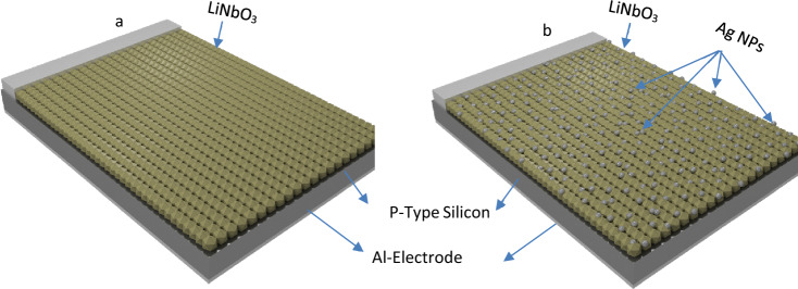
Without further purification, citric acid (CA) and ultra-pure (99.99%) niobium pentoxide were utilized. A solution was created by combining CA and ethylene glycol (EG) in a glass baker for two hours. Once it reached 90 °C, the stirring of Li2CO3 and Nb2O5 was kept for 6 h. The following materials were utilized: Li2CO3 = 3.7 g, Nb2O5 = 13.30 g, CA = 10.5 g and EG = 20 g. The molar ratio between Nb2O5 and Li2CO3 according to the procedures utilized in a previously published paper was 1:154–57. In one beaker, the ingredients were combined. The samples were made by applying a film to the quartz substrate using the CBD technique for 15 min after 12 h. The solution beaker was filled with the quartz substrate standing up. To remove the organics, all of the produced films were finally annealed at 500 °C for 2 h in a static air and oxygen environment. The photo-reduction process included a sequential immersion in AgNO3 solution followed by UV illumination58,59. By using the UV activation approach, which initially submerged the LiNbO3 thin films into a 1 M solution of AgNO3 for varying lengths of time (5, 15, 25, 35, or 45 s), Ag was added to the thin films. The film was illuminated with UV radiation from a higher value of Halogen lamp for 15 min to add the photo-reduction of silver ions to the metal. X-ray diffraction (XRD) (Schimadzu 6000)-type instrument was used to investigate the structural properties of LN. Scanning electron microscopy (SEM) (InspectTM F50) and atomic force microscopy (Angstrom advanced lnc.) were employed to examine the morphology of LN’s surface. The double-beam ultraviolet (UV)-visible spectrophotometer (Schimadzu 1800)-type equipment and Fourier transforms infrared spectroscopy (Bruker 7613)-type instrument were used to examine the optical characteristics. The exactness impedance analyzer supplied from (Agilent, 4294A, USA) was used to study the C–V properties. Figure 1 shows the schematic diagram of both heterojunction devices (LiNbO3/Si) and (Ag decoration LiNbO3/Si).
Results and discussion
structural properties
The X-ray diffraction results for pure and Ag-decorated LiNbO3 nanostructure were obtained using various immersion times. As shown in Fig. 2, the LN peaks at 2θ = 23.68°, 32.64°, 34.62°, 47.54° and 54.31° correspond to the (012), (104), (110), (024) and (116) planes, respectively60–65. Table 1 lists the structural properties of pure and Ag-decorated LN nanophotonics that must be measured. Scherrer’s formula was used to compute the crystallite size (D)66–68.
\[
D=\frac{K\lambda }{\beta \, \mathrm{cos} \, \theta }
\]
where, the constant k is assumed to be 0.94, λ is the utilized X-ray wavelength that is assumed to be 1.54 Å, and θ is the Full width at a half maximum of the X-ray diffraction pattern equal to Bragg’s angle. In order to calculate the strain (ε) and dislocation density (δ) of LN nanophotonics, the following relationships were used69–75.
\[
\delta =\frac{1}{{D}^{2}}
\]
\[
\varepsilon =\frac{\beta } {4 \,{\tan} \, \theta }.
\]
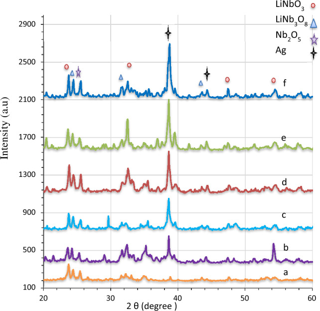
Table 1: Ag-decorated LiNbO3 nanophotonic parameters at different decorated time.
| Chemical interaction time (min) | Orientation (hkl) | Peaks (2θ) | Grain size (nm) | Dislocation Density (δ) (109) (lines/m2) | Strain (10−3) | dhkl | Lattice constants a, c |
|---|---|---|---|---|---|---|---|
| Pure | 12 | 23.75 | 102.67 | 9.48 | 0.68 | 3.76 | a = 5.1566 |
| c = 13.85 | |||||||
| 104 | 32.6 | 96.52 | 10.73 | 0.37 | 2.74 | a = 5.1566 | |
| c = 13.85 | |||||||
| 110 | 34.55 | 93.08 | 12.88 | 0.31 | 2.58 | a = 5.1566 | |
| c = 13.85 | |||||||
| 24 | 47.4 | 91.02 | 17.3 | 0.28 | 1.88 | a = 5.1566 | |
| c = 13.85 | |||||||
| 116 | 53.23 | 85.15 | 21.53 | 0.26 | 1.72 | a = 5.1566 | |
| c = 13.85 | |||||||
| 5 s | 12 | 23.68 | 95.41 | 11.45 | 0.64 | 3.74 | a = 5.1566 |
| c = 13.85 | |||||||
| 104 | 32.6 | 93.12 | 14.12 | 0.54 | 2.73 | a = 5.1566 | |
| c = 13.85 | |||||||
| 110 | 34.64 | 89.91 | 15.98 | 0.33 | 2.57 | a = 5.1566 | |
| c = 13.85 | |||||||
| 24 | 47.54 | 88.19 | 17.63 | 0.27 | 1.87 | a = 5.1566 | |
| c = 13.85 | |||||||
| 116 | 54.31 | 81.62 | 19.23 | 0.25 | 1.71 | a = 5.1566 | |
| c = 13.85 | |||||||
| 15 s | 12 | 23.74 | 93.8 | 12.98 | 0.59 | 3.75 | a = 5.1566 |
| c = 13.85 | |||||||
| 104 | 32.6 | 91.64 | 15.24 | 0.5 | 2.71 | a = 5.1566 | |
| c = 13.85 | |||||||
| 110 | 34.65 | 88.2 | 18.11 | 0.3 | 2.57 | a = 5.1566 | |
| c = 13.85 | |||||||
| 24 | 47.54 | 87.32 | 20.67 | 0.26 | 1.86 | a = 5.1566 | |
| c = 13.85 | |||||||
| 116 | 54.31 | 79.93 | 21.87 | 0.23 | 1.68 | a = 5.1566 | |
| c = 13.85 | |||||||
| 25 s | 12 | 23.75 | 92.24 | 14.45 | 0.55 | 3.74 | a = 5.1566 |
| c = 13.85 | |||||||
| 104 | 32.61 | 89.24 | 16.27 | 0.46 | 2.7 | a = 5.1566 | |
| c = 13.85 | |||||||
| 110 | 34.65 | 84.85 | 19.68 | 0.29 | 2.54 | a = 5.1566 | |
| c = 13.85 | |||||||
| 24 | 47.55 | 83.98 | 22.49 | 0.25 | 1.91 | a = 5.1566 | |
| c = 13.85 | |||||||
| 116 | 54.32 | 77.87 | 23.72 | 0.23 | 1.68 | a = 5.1566 | |
| c = 13.85 | |||||||
| 35 s | 12 | 23.76 | 88.12 | 15.14 | 0.42 | 3.74 | a = 5.1566 |
| c = 13.85 | |||||||
| 104 | 32.61 | 85.96 | 16.89 | 0.33 | 2.73 | a = 5.1566 | |
| c = 13.85 | |||||||
| 110 | 34.65 | 81.85 | 20.19 | 0.27 | 2.57 | a = 5.1566 | |
| c = 13.85 | |||||||
| 24 | 47.57 | 78.99 | 23.11 | 0.24 | 1.87 | a = 5.1566 | |
| c = 13.85 | |||||||
| 116 | 54.36 | 76.61 | 24.29 | 0.22 | 1.71 | a = 5.1566 | |
| c = 13.85 | |||||||
| 45 s | 12 | 23.7 | 86.32 | 16.91 | 0.35 | 3.75 | a = 5.1566 |
| c = 13.85 | |||||||
| 104 | 32.62 | 83.68 | 18.25 | 0.31 | 2.7 | a = 5.1566 | |
| c = 13.85 | |||||||
| 110 | 34.55 | 80.97 | 22.68 | 0.25 | 2.55 | a = 5.1566 | |
| c = 13.85 | |||||||
| 24 | 47.75 | 76.56 | 23.17 | 0.23 | 1.88 | a = 5.1566 | |
| c = 13.85 | |||||||
| 116 | 53.24 | 73.85 | 25.37 | 0.21 | 1.67 | a = 5.1566 | |
| c = 13.85 |
Bragg’s formula was used to compute the interplanar distance (d) for the all sets of LN nanophotonics76–79.
\[
d=\frac{n}{2 \, \mathrm{ sin \, \theta }},
\]
where, n is a positive integer number, and d is the value provided in Table 1. Two phases of LN with a polycrystalline structure may be identified in nanophotonics, i.e. LN and LiNb3O8 phases. The LN phase is preferable. However, the achieved phase is oriented at (012). From the XRD results, a small amount of secondary lithium-deficient phase (LiNb3O8) is clearly observed in the all samples. This phase is produced through the oxygen–LiNbO3 interfacial interaction. The XRD peaks of LiNb3O8 are at 2θ = 24.45, 31.10, 35.20, 43.47 corresponding to the (400), (202), (− 601), (203) and planes, respectively. These results agree with the Joint Committee on Powder Diffraction Standards (JCPDS) card no. 01-074-2239. Notably, the different peaks (Nb2O5) occur at 2θ = 25.55, which corresponds to the (− 212) plane. This result concurs with JCPDS card no. 01-074-2239).
The diffraction peaks of nano silver at 2θ = 38.2, which corresponds to the (111) diffraction plane, as portrayed in Fig. 2, might be used to identify the presence of silver atoms on the LiNbO3 nanostructure. In spite of the presence of the main phases related to LiNbO3 nanostructure, their intensities demonstrated a consistent lowering with an increase in the silver incorporation. A notable diffraction peak connected to the (200) diffraction plane could be seen. The Ag nanoparticles at 2θ = 44.3 diffraction angle account for this peak80.
According to a previous study, a rise in the peak intensities assures that the Ag nanoparticles are incorporated into the base material’s lattice52. Table 1 indicates that the experimental values and measured lattice constants are similar81.
Optical properties
The optical properties results for pure and Ag decorated LiNbO3 nanostructure using various immersion times (5, 15, 25, 35, 45 s) are illustrated in Fig. 3. The absorption peaks ranging from 350 to 400 nm at the region of UV are one of the unique characteristics of the LiNbO3 nanostructure, and this result confirms the results of X-ray diffraction (XRD) shown previously. The optical absorbance increases by 50% as the number of the nanoparticles of silver are growing by adjusting the immersion period, as depicted in Fig. 3. The increases in the silver (Ag) decorating time are seen at 400 nm and might be attributed to the plasmonic effect. Also, this was ascribed to the charge transfer transition between the electrons of Ag and LiNbO3 which could reduce the band gap energy between the conduction band and the valence band of LiNbO3, and the Ag nanoparticles on LiNbO3 can trap the electrons resulting in prevention of the electron hole recombination82.
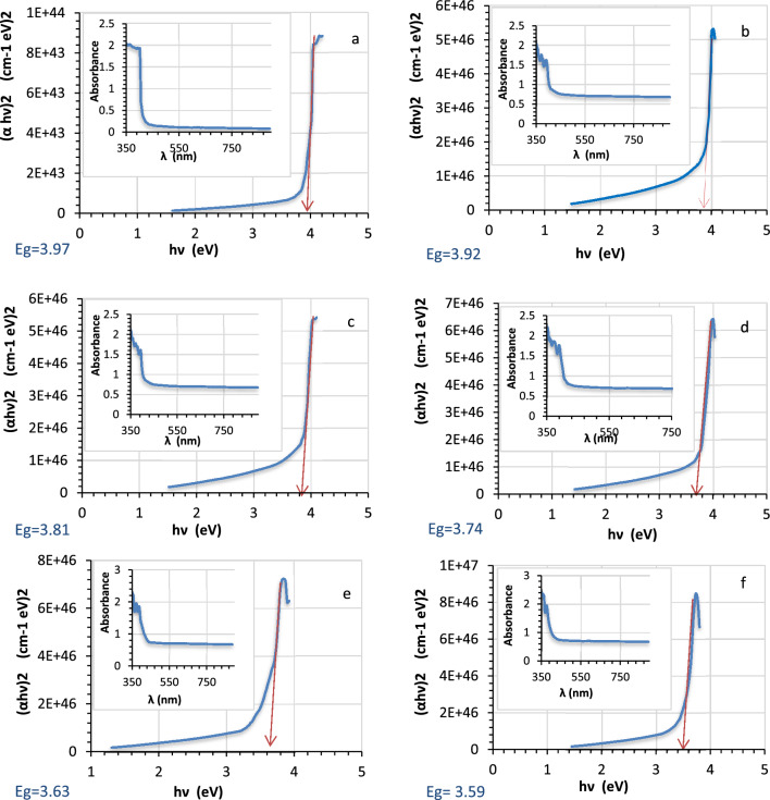
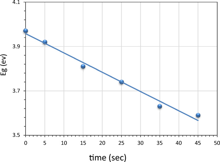
The calculated energy gap is revealed against the immersion time in Fig. 4. One observes that the energy gap of LiNbO3 was 3.97 eV. After Ag decoration LiNbO3, the band gap energy was reduced to 3.59 eV. It is clear that the effects of the quantum confinement in the films cause the optical energy gap to narrow with increasing the Ag (silver) concentration. With added silver, the band gap energy drops. Since the LiNbO3‘s conduction band edge may experience a band bending due to the close contact between the Ag nanoparticles and the host material, a reduction in the optical band gap energy of LiNbO3 is anticipated to occur83.
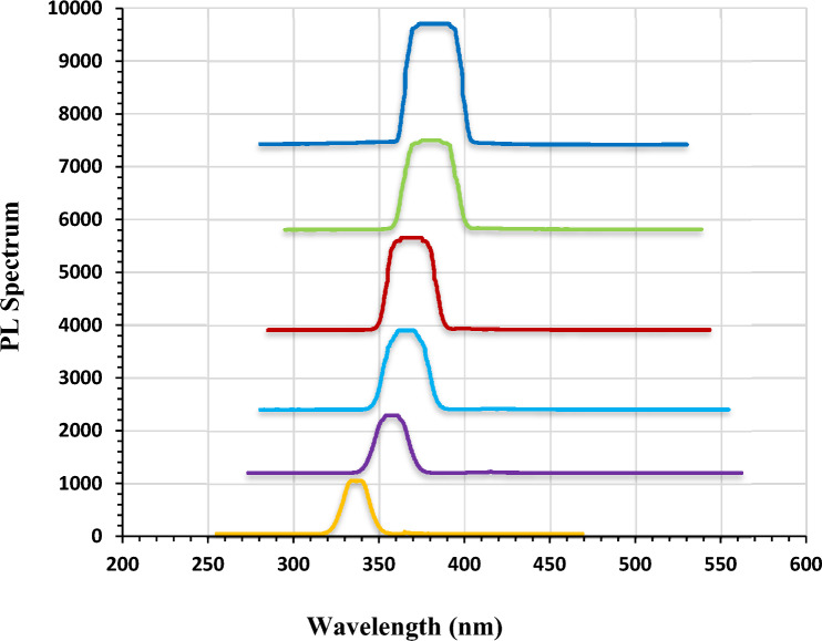
PL measurements results
The photoluminescence (PL) spectra of the pure and Ag-decorated LiNbO3 nanostructure grown on the quartz substrate at different immersion times are displayed in Fig. 5. The PL peaks are observed at around 335 (for pure LiNbO3), 358 (for 5 s Ag-decorated LiNbO3), 360 (for 15 s Ag-decorated LiNbO3), 363 (for 25 s Ag-decorated LiNbO3), 371(for 35 s Ag-decorated LiNbO3) and 476 (for 45 s Ag-decorated LiNbO3) in the visible region of the electromagnetic spectrum. These are consistent with the X-ray diffraction (XRD) results and the optical properties which are shown previously. The emission intensity is significantly weakened in pure LiNbO3 compared to the decorated films, and the band shifts slightly towards the higher wavelength region. This is attributed to the band to band transition of electrons from the conduction band to the valence band. This indicates that the recombination rate of photo-generated carriers increased when doping with Ag. These results agree with84.
Morphological studies
SEM was used to determine the surface morphology of the LiNbO3 nanostructure surface at various immersion times for the pure and Ag-decorated LiNbO3 nanostructures, as manifested in Fig. 6a–e. The pure LiNbO3 nanostructure in Fig. 6a views the smooth and homogenous structure. The crystalline size was calculated from the FESEM image and was about 100–110 nm for pure LiNbO3 and around 95, 90, 85, 80, and 75 nm for Ag decoration LiNbO3 at 5, 15, 25, 35, and 45 s respectively. The number of Ag nanoparticles rises with the doping time of the final immersion periods, as seen in Fig. 6b–f. The measured structural characteristics concur with this. Their sizes and shapes were consequently changed. As nanoparticles possess a larger surface area in comparison with their volume, their surface energies are high and these particles agglomerate to reduce the excessive surface energies and reach a thermodynamic stability condition. The agglomeration process is majorly occurring as a result of Van der Waals attraction52,85. It was found that with increasing the immersion time, especially at 45 s, a change in the particle morphology and size occurs, as evinced in Fig. 6. Small spherical grains that are part of the Ag nanoparticles are submerged for shorter periods of time, whereas the creation of the Ag nanorods may be detected after 45 s. This may be due to the sliver spot can be localized at the top end of growing nanorods called the tip growth process. This can follow the vapor–liquid–solid (VLS) mechanism.
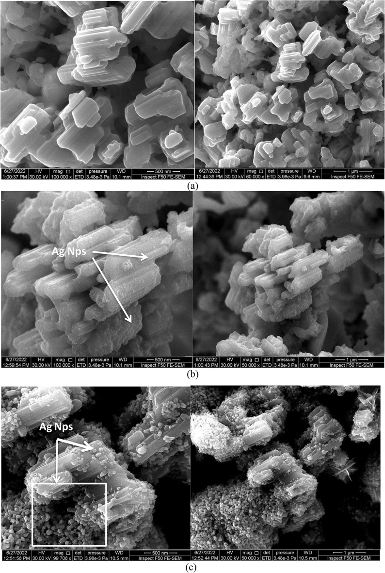
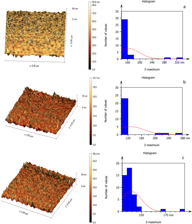
Figure 7 portrays the AFM pictures of the LiNbO3 nanophotonics, which have a surface with a homogeneous density and demonstrate a reduction in grain size with increasing immersion duration86. The LiNbO3 nanophotonics’ surface topography, as elucidated in the AFM micrographs, demonstrates that the grains are evenly dispersed across the scanning region. LiNbO3 topographical images were not significantly changed when decorated by silver (Ag) nanostructures that was due to the sparsed distribution of the small spherical silver nanoparticles within LiNbO3 nanostructure outermost layers. However, the histograms revealed more obvious results. On the other hand, it was noted that the surface roughness decreases from 80.71 to 23.02 nm as the immersion time is increased. The root mean square also decreases from 91.61 to 28.14 nm. Increasing the Ag decoration levels leads to a decreasing in the root mean square to reach a minimum value of 28.14 nm at 45 s. According to this result, the reduction in the surface roughness in the Ag decoration levels may be attributed to the decrease of LiNbO3 grain size, which was discussed previously, and this result is in a good agreement with27.
Fourier transform infrared spectroscopy
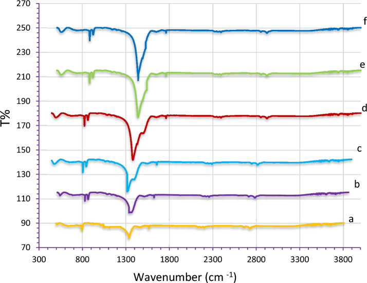
The FTIR spectra of pure LiNbO3 and Ag-decorated LiNbO3 are shown in Fig. 8. These results showed that LiNbO3, grown crystal were homogeneous in composition. The figure shows the infrared spectra of different immersion time in AgNO3. It can be observed that the band at 515 cm−1 is related to specific vibration of Li–O bonds. Also can be observed in all samples that the band 871 cm−1 is assigned to Nb–O–Nb stretching vibration87. The absorption peaks at 1470 cm−1 are assigned to bending vibration of surface adsorbed water molecules. From the results, we notice that the bonds between the materials are formed. No bands associated with the additional phases of AgO or AgO2 are visible in FTIR spectra, which points to the great purity of the produced materials. A noticeable increase in the intensity of the peaks of samples doping with Ag Nps. The change of O–H stretch absorption intensity in the composite sample is attributed to the interactions between silver ions and hydroxyl group of LN and may be attributed to presence of Ag nanoparticles due to the effect of surface plasmon resonance (SPR), this results agree with88.
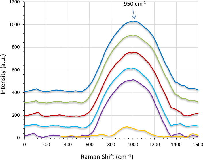
Raman spectra measured
Figure 9 illustrates the Raman spectra with the wave numbers ranging from 200 to 1000. The peaks for pure LiNbO3 were observed at 258, 410, 510, 745 and 830 cm−1 and were attributed to the LN phonon mode E transverse optical (TO). After being decorated with AgNPs, it was noticed that the peaks shifted to a higher intensity due to the plasmonic effect of Ag nanoparticles. To explain that, the Raman enhancement occurred as a result of the hot spot’s impact. The hot spots stand for the gaps between the metallic nanoparticles, when exposed to a ram of an incident source, exhibit high intense bands due to the enhanced electric field resulting from the plasmonic effect of Ag nanoparticles. This can be clearly noted for the band observed in the wave number region exceeding 1000 cm−1 that might be belong to Ag.
Resistance (R) with temperature (T)
Figure 10 views the resistance (R) of pure and Ag-decorated Lithium niobate as a function of temperature which was measured by Kiethly electrometer. Each sample was placed on a plate under which a furnace like structure was equipped. The first reading for all the samples was taken under thermal equilibrium condition (at room temperature) to test the resistance of LiNbO3 nanostructure prepared with different films’ thicknesses. The minimum obtained resistance was about 45 kΩ. Two point’s probes were attached to the metalized zones. The range of temperature began from the room temperature up to 200 °C. The relative resistance of all samples decreases continuously with increasing temperature after being decorated with silver nanoparticles. Such behaviour can be attributed to the increasing electrical conductivity with increasing temperature due to the electron transition from the valence band to the conduction band50.
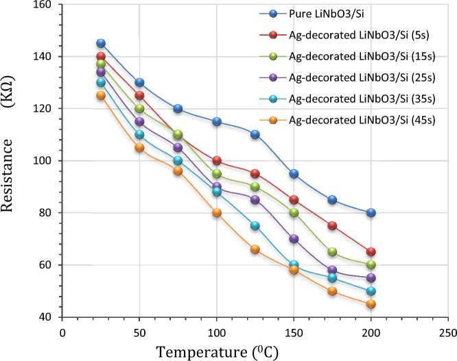
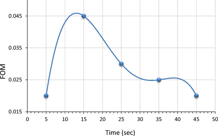
Figure of merit of Ag at LiNbO3 nanostructure
Figure 11 depicts the figure of merit (F.O.M.) of LiNbO3 thin films prepared after multi-optimization steps. Different immersion times were used to prepare Ag at the LiNbO3 nanostructure sample. The applicability of prepared films in optoelectronic devices could be quantified by the optimal combination of high electrical conductivity and high absorption of visible light, and the figure of merit (ɸ) can be calculated by applying89,90:
\[
\phi = {1}/\alpha \rho ,
\]
where, α refers to the absorption coefficient, and ρ is the electrical resistivity. The figure of merit used in judging the quality of the immersion time for the prepared films can be observed in Fig. 11 that shows the changing of the figure of merit with the immersion time, and it was found that the best immersion time is at 15 s.
Electrical properties of LiNbO3/ Si and Ag decorated LiNbO3/Si heterojunction device
Current–voltage (I–V) measurement
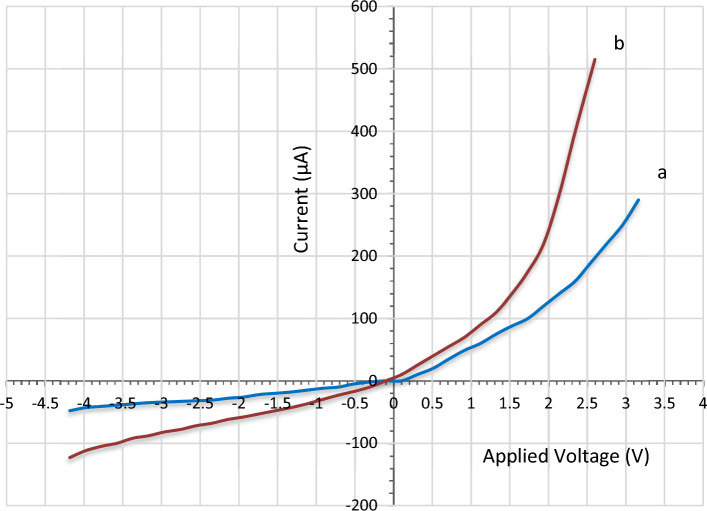
The influence of adding of silver NPs on the optoelectronic characteristics of the LiNbO3 nanostructure nano-films was determined via using the Ag-decorated LiNbO3/Si heterojunction device at the optimum condition. Each of the two devices shows a normal diode operation in both forward and reverse biasing within a rectifying mode. However, the silver-decorated based photodetector showed enhanced forward characteristics. The results were compared with those corresponding to the undecrated LiNbO3/Si material. The measurements of I–V in the forward and reverse bias were carried under the dark condition and after doping by heterojunction devices shown in Fig. 12. The two devices depicted the rectifying properties. It is evident that there are two reverse current zones on the I–V curve. The first is the generation zone, where the reverse current marginally rises with the applied voltage and produces electron–hole pairs at low bias. As the reverse bias increases in the second zone, a large rise may be seen. The reverse current of the Ag-decorated LiNbO3/Si heterojunction was found to be increased slightly after decoration due to decreasing the resistivity of LiNbO3. Two regions are recognized in the I–V characteristics in the forward bias case. The first region represents the recombination current under low voltage, as it is produced when the number of carriers created exceeds the number of self-charging carriers, which occurs when the valence electrons and holes recombine in the conduction band. The mass action law of (nxp > ni2) is not valid. The second region, which clearly shows an increase in forward current, indicates the propagation region or the bending under high voltages. For LiNbO3/Si heterojunction decorated with Ag, the current could be seen to increase, which is related to decreasing the resistivity of LiNbO3 nanostructure compared to the undecorated heterojunction. In fact, the generated dark current comes from the leakage current than passing on the surface of the heterojunction91. The ideality factor was found to be around (3.1 and 2.6) for the LiNbO3/Si and Ag-decorated LiNbO3/Si heterojunction device, respectively. The ideality factors were both higher than the ideal value (1) indicating for non-ideality operation of the pn-heterojunction based photodetector. This can be attributed to the mechanism of tunneling, LiNbO3 crystal defects including oxygen vacancies, mismatching between the lattice of LiNbO3 and the silicon based wafer, and disorder in surface morphologies52. The lower value belonged to the Ag decorated LiNbO3 can be as a result of the enhanced built-in potential and barrier height (as the barrier height is inversely proportional to the ideality factor). In addition, as the ideality factor for (Ag decorated LiNbO3) was lower than (2), then the transporting process was controlled by the thermionic emission. These values are better than the reported ideality factors in Ref. 52. The large ideality factor value confirms the presence of the surface states at the LiNbO3/Si interface. Decreasing the ideality factor after doping can be explained due to the compensation effect achieved by Ag decoration which decreases the role of the surface trap.
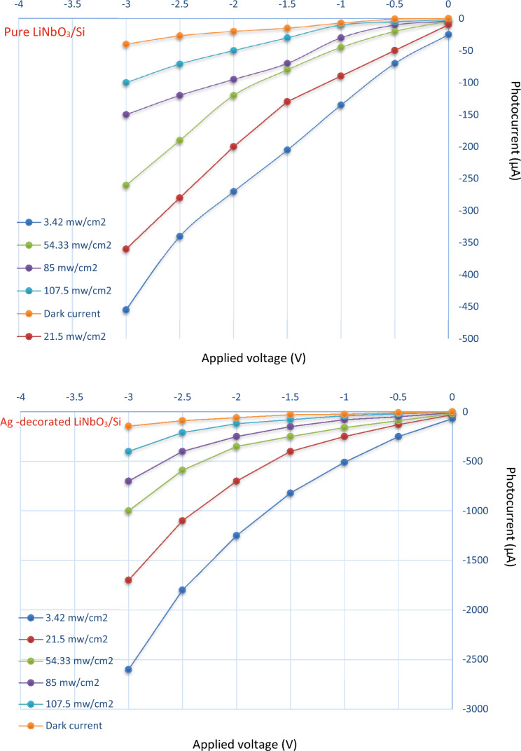
The illuminated I–V characteristics at different illumination intensities are revealed in Fig. 13. The generation of the pairs of electrons-halls in the zone of the depletion and diffusion length is responsible for the rise in photo-current in the reverse bias direction. This occurred when the energy of incident light is greater or equal to the energy gap of LiNbO3. The Ag-decorated LiNbO3/Si photodetector’s structure depicts a clear improvement in the photocurrent. This improvement is connected to the optical absorption’s plasmonic impact, which increased the absorption of photons as well as due to widening the depletion layer width owing to the doping effect.
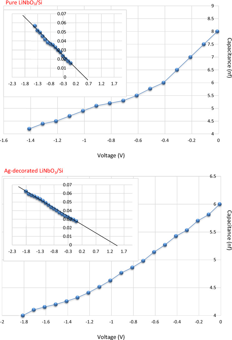
Capacitance–voltage characteristics
These properties are essential to the definition of parameters, such as the built-in potential, and the type of the junction. The capacitance (C) is inversely dependent on the reverse bias (Fig. 14). It is clear from this figure that the junction capacitance decreases with the increase of the bias voltage due to increasing of the width of the depletion region. The junction capacitance decreases after the Ag decoration due to the widening of the depletion layer width of the heterojunction. The insert charts of the built-in potential (Vbi) value of the LiNbO3/Si and Ag-decorated LiNbO3/Si heterojunction is displayed also in this figure. The value of the built-in potential (Vbi) was calculated by extrapolating and interception of the straight part of the curve to the zero point of 1/C2. The value of Vbi was found to be 0.6 for LiNbO3/Si and 1.35 for Ag-decorated LiNbO3/Si which agree with92. As observed from this figure, the Vbi value increased after the Ag decoration from 0.6 to 1.35 confirming the improvement in the junction properties.
Spectral responsivity (Rλ) measurement
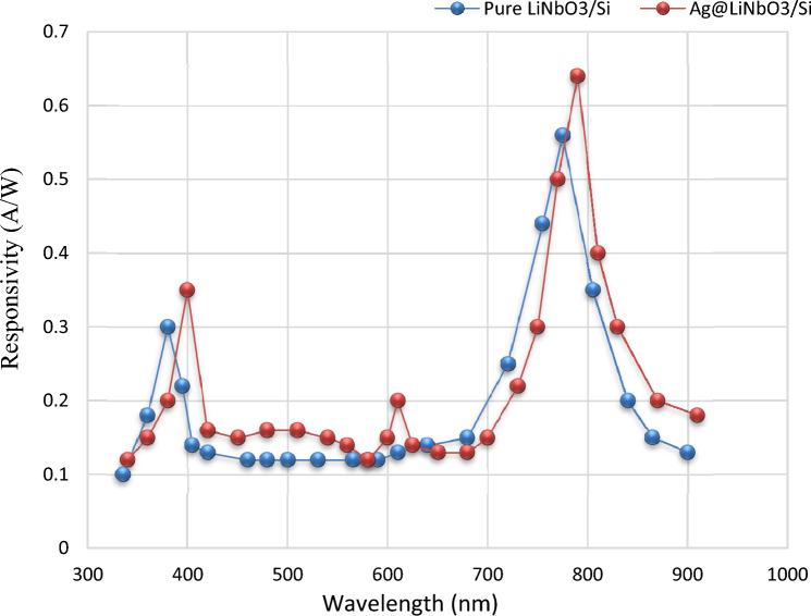
The plot of spectral responsivity (Rλ) as a function of wavelength for LiNbO3/Si and Ag-decorated LiNbO3/Si heterojunction photo-detector is manifeted in Fig. 15. The increase in responsivity after the decoration with Ag is correlated to the rise in photocurrent arising from increasing the depletion layer width. A slight shifting in the peak response (red shift) towards the long wavelength region could be noticed after the Ag decoration due to the surface Plasmon response (SPR) of Ag. Due to the high absorption coefficient and the band gap of the LiNbO3 film, there is a noticeable improvement in responsiveness in the shorter wavelength area. The first small peak was observed at 375 nm due to the absorption edge of the LN films. It may be possible to detect a shift in the peak response at 400 nm, which is connected to a shift in the energy gap for a certain Ag concentration in the direction of the visible spectrum. The second peak was discovered at 790 and related to an increase in the active layer’s absorption coefficient brought on by the plasmonic characteristics of the inserted metal. After 900 nm, the low responsivities can be observed as a result of the reduced carriers’ concentrations probabilities. The responsivity of the LiNbO3/Si device decorated with Ag was also improved, which may be related to the light absorbed in the depletion region of the silicon substrate93–95. Since the minority carrier’s diffusion length is away from the junction interface (depletion zone), these wavelengths are absorbed. In this instance, the incident photon energy’s product e–h pairs shift in accordance with the internal electrical field. As a result, the likelihood of carrier concentration might be decreased, which results in lesser responsiveness. On the other hand, the SPR of Ag enhanced the responsivity in visible region around 600 nm.
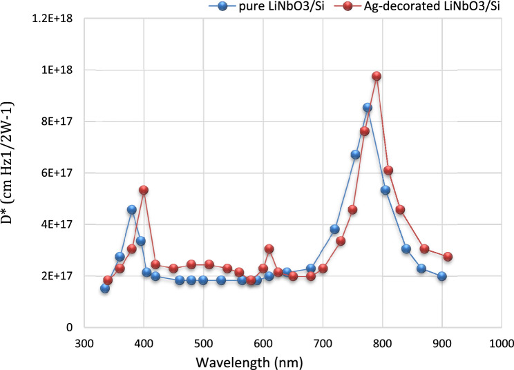
Specific detectivity (Dλ*)
Specific detectivity is a very significant parameter which describes the performance of the photo-detector and its ability to detect the weak signal96. The detectivity for this device was calculated by using equation97–101:
\[
{\text{D}}* = {\text{ R}}\lambda \, \left( {{\text{A}}.\Delta {\text{f}}} \right)^{{{1}/{2}}} /{\text{I}}_{{\text{n}}} ,
\]
\[
{\text{In}} = \, \left( {{\text{2q I}}_{{\text{d}}} .\Delta {\text{f}}} \right)^{{{1}/{2}}} ,
\]
where, (Δf): is the frequency band width, (Id) is the dark current, and (In) is the noise current. The specific detectivity of the photo-detector depends on the noise current and responsivity. Figure 16 portrays the plot detectivity versus the wavelength for LiNbO3/Si and Ag-decorated LiNbO3/Si photo-detectors. These figures demonstrate that the detectivity plot is similar to that of responsivity plot. The obtained values of detectivity for the LiNbO3/Si and Ag-decorated LiNbO3/Si photo-detectors are in the UV visible region. The high detectivity of the device indicates that the photo-detector has low noise, dark current or high responsivity. Enhancement of the detectivity of photo-detector may be attributed to increasing the detector responsivity, decreasing the concentration of structural defects, and decreasing the leakage current102.
Quantum efficiency (QE)
Quantum efficiency can be defined as the ratio between the numbers of generating electron to the incident photon103. Figure 17 evinces the quantum efficiency versus the wavelength spectral for the pure LiNbO3/Si and Ag decorated LiNbO3/Si photo-detectors. Quantum efficiency was estimated by the equation104–107:
\[
{\text{Q }} = { 1}.{\text{24 R}}_{\lambda } /\lambda \, \left( {\mu {\text{m}}} \right).
\]
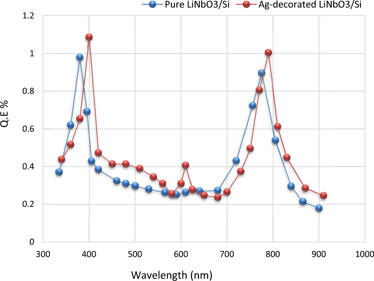
The highest value was at a (390 nm) wavelength for Ag decorated LiNbO3/Si and at a (375 nm) wavelength for LiNbO3/Si photo-detector. The value of obtained quantum efficiency is larger or comparable to the wide band gap silicon-based heterojunction98–111. The enhancement was due to the incorporation of silver (Ag) noble metallic nanoparticles that induced a plasmonic effect leading to higher extraction of electrons generated via incident photon.
Conclusion
At various doping periods, the effects of incorporating silver nanoparticles (Ag) on the structural, optical, morphological, and electrical characteristics of LiNbO3 nanostructure were investigated. In comparison to the pure LiNbO3 film, the SEM pictures showed a dense distribution of grains with novel structure at a higher time of 45 s. In this study, ornamented Ag significantly boosted and improved the device photoresponse and photocurrent.
Supplementary Materials
References
- MA Fakhri, U Hashim, ET Salim, ZT Salim. Preparation and charactrization of photonic LiNbO3generated from mixing of new raw materials using spry pyrolysis method. J. Mater. Sci. Mater. Electron., 2016. [DOI]
- D Janner, D Tulli, M Jofre, D Yudistira, S Balsamo, M Belmonte, V Pruneri. Domain inverted acousto- and electrooptic devices and their application to optical communication, sensing, laser sources, and quantum key distribution. IEEE J. Sel. Top. Quantum Electron., 2013. [DOI]
- MA Fakhri, Y Al-Douri, ET Salim, U Hashim, Y Yusof, EB Choo, ZT Salim, YN Jurn. Structural properties and surface morphology analysis of nanophotonic LINBO3. ARPN J. Eng. Appl. Sci., 2016
- P Kumar, SM Baru, S Perero, RML Sai, I Bhamik, S Ganesamoorthy, AK Karnal. X-ray photoelectron spectroscopy, high-resolution X-ray direction and refractive index analyses of Ti-doped lithium niobate (Ti:LiNbO3) nonlinear optical single crystal. J. Phys., 2010
- Z Vakulov, E Zamburg, D Khakhulin, A Geldash, DA Golosov, SM Zavadski, AV Miakonkikh. Oxygen pressure influence on properties of nanocrystalline LiNbO3 films grown by laser ablation. Nanomaterials, 2020. [DOI | PubMed]
- ZT Salim, U Hashim, MKM Arshad, MA Fakhri, ET Salim. Zinc oxide flakes-corolla lobes like nano combined structure for SAW applications. Mater. Res. Bull., 2017. [DOI]
- R Barik, SK Satpathy, B Behera, SK Biswal, RK Mohapatra. Synthesis and spectral characterizations of nano-sized lithium niobate (LiNbO3) ceramic. Micro Nanosyst., 2020. [DOI]
- CR Cena, GB Torsoni, GQD Freitas. Synthesis of LiNbO 3 thin films by using niobium oxalate. Matéria (Rio de Janeiro), 2016. [DOI]
- ZT Salim, U Hashim, MKM Arshad, MA Fakhri, ET Salim. Frequency-based detection of female Aedes mosquito using surface acoustic wave technology: Early prevention of dengue fever. Microelectron. Eng., 2017. [DOI]
- B Knabe, D Schutze, T Jungk, M Svete, W Assenmacher, W Mader, K Buse. Synthesis and characterization of Fe-doped LiNbO3 nanocrystals from a triple-alkoxide method. Phys. Status Solidi (A), 2011. [DOI]
- 11.Tulli, D. Micro-nano structured electro-optic devices in LiNbO3 for communication and sensing. (2012).
- MA Fakhri, ET Salim, MHA Wahid, U Hashim, ZT Salim, RA Ismail. Synthesis and characterization of nanostructured LiNbO3 films with variation of stirring duration. J. Mater. Sci. Mater. Electron., 2017. [DOI]
- J Zhang, X Zhang. Biomolecular binding dynamics in sensors based on metallic photonic crystals. Opt. Commun., 2014. [DOI]
- H Lu, B Sadani, G Ulliac, N Courjal, C Guyot, J-M Merolla, M Collet, FI Baida, M-P Bernal. 6-Micron interaction length ctro-optic modulation based on lithium niobate photonic crystal cavity. Opt. Express, 2012. [DOI | PubMed]
- MA Fakhri, ET Salim, MHA Wahid, U Hashim, ZT Salim. Optical investigations and optical constant of nano lithium niobate deposited by spray pyrolysis technique with injection of Li2CO3and Nb2O5 as raw materials. J. Mater. Sci. Mater. Electron., 2018. [DOI]
- H Chen, T Lv, A Zheng, Y Han. Discrete diffraction based on electro-optic effect in periodically poled lithium niobate. Opt. Commun., 2013. [DOI]
- P Ganguly. Semi-analytical analysis of lithium niobate photonic wires. Opt. Commun., 2012. [DOI]
- Y Al-Douri, MA Fakhri, A Bouhemadou, R Khenata, M Ameri. Stirrer time effect on optical properties of nanophotonic LiNbO3. Mater. Chem. Phys., 2018. [DOI]
- AA Mohamed, MA Metawe’e, ANZ Rashed, AIM Bendary. Ultra high speed semiconductor electrooptic modulator devices for gigahertz operation in optical communication systems. Int. J. Opt. Appl., 2011
- Y Al-Douri, MA Fakhri, N Badi, CH Voon. Effect of stirring time on the structural parameters of nanophotonic LiNbO3 deposited by spin-coating technique. Optik, 2018. [DOI]
- KS Kaur, AZ Subramanian, YJ Ying, DP Banks, M Feinaeugle, P Horak, V Apostolopoulos, CL Sones, S Mailis, RW Eason. Waveguide mode filters fabricated using laserinduced forward transfer. Opt. Express, 2011. [DOI | PubMed]
- 22.Gong, S., Song, Y.H., Manzaneque, T., Lu, R., Yang, Y., Kourani, A. Lithium niobate MEMS devices and subsystems for radio frequency signal processing. In 2017 IEEE 60th International Midwest Symposium on Circuits and Systems (MWSCAS) IEEE, 45–48 (2017).
- Y Qi, Y Li. Integrated lithium niobate photonics. Nanophotonics, 2020. [DOI]
- W Branch. Investigation of a solid-state tuning behavior in lithium niobate. IEEE Trans. Ultrason. Ferroelectrics Freq. Contr., 2020. [DOI]
- ET Salim, JA Saimon, MK Abood, MA Fakhri. Effect of silicon substrate type on Nb2O5/Si device performance: An answer depends on physical analysis. Opt. Quant. Electron., 2020. [DOI]
- J Dai, R Xu, YS Lin, CH Chen. Tunable electromagnetic characteristics of suspended nanodisk metasurface. Opt. Laser. Technol., 2020
- MA Fakhri, FG Khalid, ET Salim. Influence of annealing temperatures on Nb2O5nanostructures prepared using pulsed laser deposition method. J. Phys Conf. Ser., 2021. [DOI]
- PK Anand Prem, A Chakrapani. A millimeter-wave generation scheme based on frequency octupling using LiNbO3 mach–zehnder modulator. Natl. Acad. Sci. Lett., 2019. [DOI]
- ET Salim, R Mahmood, FG Khalid, U Hashim. Using the PLD method: Investigation of the influence of laser wavelengths on the optical morphological and structural findings of LiNbO3 nano-photonic films. Defect Diffus. Forum, 2022. [DOI]
- BS Tang, CX Sun. Adjustment for mid-infrared narrowband filtering characteristics in multilayer graphene nanofilms. Opt. Precis. Eng., 2019
- PJ Turner. 5 GHz band n79 wideband microacoustic filter using thin lithium niobate membrane. Electron. Lett., 2019. [DOI]
- ZT Salim, U Hashim, MKM Arshad, MA Fakhri. Simulation, fabrication and validation of surface acoustic wave layered sensor based on ZnO/IDT/128° YX LiNBO3. Int. J. Appl. Eng. Res., 2016
- M Bazzan, C Sada, M Bazzan, C Sada. Optical waveguides in lithium niobate: Recent developments and applications. Appl. Phys. Rev., 2015. [DOI]
- I Bolesta, M Vakiv, V Haiduchok, O Kushnir, R Gamernyk. Optical properties of LiNbO3-Ag nanocomposites. Int. Conf. Oxide Mater. Electron. Eng., 2018
- MK Abood, ET Salim, JA Saimon. Niobium pentoxide thin film prepared using simple colloidal suspension for optoelectronic application. Int. J. Nanoelectron. Mater., 2018
- MS Alwazny, RA Ismail, ET Salim. High-quantum efficiency of Au@LiNbO3 core–shell nano composite as a photodetector by two-step laser ablation in liquid. Appl. Phys. A, 2022. [DOI]
- JA Garibay-Alvarado, R Farías, SY Reyes-López. Sol-gel and electrospinning synthesis of lithium niobate-silica nanofibers. Coatings, 2019. [DOI]
- M Liu, D Xue, K Li. Soft-chemistry synthesis of LiNbO3 crystallites. J. Alloy. Compd., 2013. [DOI]
- MA Fakhri. Annealing effects on opto-electronic properties of Ag2O films growth using thermal evaporation techniques. Int. J. Nanoelectron. Mater., 2016
- X Wang, Y Liang, S Tian, W Man, J Jia. Oxygen pressure dependent growth of pulsed laser deposited LiNbO3 films on diamond for surface acoustic wave device application. J. Cryst. Growth, 2013. [DOI]
- F Meriche, A Boudrioua, R Kremer, E Dogheche, E Neiss-Clauss, R Mouras. Fabrication and investigation of 1D and 2D structures in LiNbO3 thin films by pulsed laser ablation. Opt. Mater., 2010. [DOI]
- A Tanaka, K Miyashita, T Tashiro, M Kimura, T Sukegawa. Preparation of lithium niobate films by metalorganic chemical vapor deposition with a lithium alkoxide source. J. Cryst. Growth, 1995. [DOI]
- D Callejo, V Bermudez, MD Serrano, E Diéguez. Lithium niobate films on periodic poled lithium niobate substrates prepared by liquid phase epitaxy. J. Cryst. Growth, 2002. [DOI]
- MA Fakhri, Y Al-Douri, A Bouhemadou, M Ameri. Structural and optical properties of nanophotonic LiNbO 3 under Stirrer time effect. J. Opt. Commun., 2017. [DOI]
- V Iyevlev, A Kostyuchenko, M Sumets, V Vakhtel. Electrical and structural properties of LiNbO3 films, grown by RF magnetron sputtering. J. Mater. Sci. Mater. Electron., 2011. [DOI]
- VG Deon, A Thesing, LR Santana, VC Costa, MO Vaz, RM Silva. Synthesis of LiNbO3 nanocrystals by microwave-assisted hydrothermal method: Formation mechanism and application to hydrogen evolution reaction. Chem. Pap., 2021. [DOI]
- MA Fakhri, ET Salim, U Hashim, AW Abdulwahhab, ZT Salim. Annealing temperature effect on structural and morphological properties of nano photonic LiNbO3. J. Mater. Sci. Mater. Electron., 2017. [DOI]
- 48.Arivanandhan, M., Ekpunobi, A.,Yasuhiro, H. Effect of deposition time on the chemical bath deposition method of ZnO thin films. In AIP Conference Proceedings (2013).
- 49.Zainuddin, L. W., Samat, M. H., Zaki, N. H. M., Badrudin, F. W., Osman, N., Jani, A. M. M., et al. Electronic and optical properties of Au and Ag doped LiNbO3 from first principles study. Mater. Today Proc. (2023).
- MK Abood, ET Salim, JA Saimon, AA Hadi. Electrical conductivity, mobility and carrier concentration in Nb2O5 films: Effect of NH4OH molarity. Int. J. Nanoelectron. Mater., 2021
- SV Boriskina, H Ghasemi, G Chen. Plasmonic materials for energy: From physics to applications. Mater. Today, 2013. [DOI]
- ET Salim, SR Shafeeq, MJ AbdulRazzaq, MA Fakhri, SC Gopinath. Photo-activation of Ag chemicals for enhanced Nb2O5 optoelectronic device employing plasmonic effects. Surf. Interfaces, 2023. [DOI]
- M Sturaro. Degenerately doped metal oxide nanocrystals as plasmonic and chemoresistive gas sensors. ACS Appl. Mater. Interfaces, 2016. [DOI | PubMed]
- RB Fadhil, ET Salim, WK Khalef, FH Alsultany. Deposition time effect on LN films properties using chemical bath deposition method without post heat treatment. Int. J. Nanoelectron. Mater., 2022
- MA Fakhri, Y Al-Douri, U Hashim. Fabricated optical strip waveguide of nanophotonics lithium niobate. IEEE Photonics J., 2016. [DOI]
- RB Fadhil, ET Salim, WK Khalef. LiNbO3 thin films at different stirrer time: Synthesis using chemical bath deposition (CBD) method. J. Mater. Sci. Mater. Electron., 2022. [DOI]
- RB Fafhil, ET Salim, WK Khalef. Synthesis of LiNbO3 microstructures: Structural, optical, and surface morphology using chemical bath deposition (CBD) method without post-heat treatment. Egypt. J. Chem., 2023. [DOI]
- ET Salim, JA Saimon, MK Abood, MA Fakhri. Some physical properties of Nb2O5 thin films prepared using nobic acid based colloidal suspension at room temperature. Mater. Res. Express, 2017. [DOI]
- 59.Afsheen, S., Shahzadi, K., Iqbal, T., Zafar, M., Saleem, R., Sayed, M. A., et al. A chyranthes aspera-based biosynthesis of silver nanoparticles to investigate the efficacy against mosquito larvae. Biomass Convers. Biorefinery. 1–10 (2022).
- L Zhu. High-performance Cu nanoparticles/threedimensional graphene/Ni foam hybrid for catalytic and sensing applications. Nanotechnology, 2018. [DOI | PubMed]
- MA Fakhri, ET Salim, AW Abdulwahhab, U Hashim, ZT Salim. Optical properties of micro and nano LiNbO3 thin film prepared by spin coating. Opt. Laser Technol., 2018. [DOI]
- YJ Wang, W Long, L Wang, R Yuan, A Ignaszak, B Fang, DP Wilkinson. Unlocking the door to highly active ORR catalysts for PEMFC applications: Polyhedron-engineered Ptbased nanocrystals. Energy Environ. Sci., 2018. [DOI]
- L Xiong. Biogenic synthesis of Pd-based nanoparticles with enhanced catalytic activity. ACS Appl. Nano Mater., 2018. [DOI]
- MA Fakhri, M Halim, A Wahid, SM Kadhim, BA Badr, ET Salim, U Hashim, ZT Salim. The structure and optical properties of Lithium Niobate grown on quartz for photonics application. Eur. Phys. J. Conf., 2017. [DOI]
- JM Gichumbi, HB Friedrich. Half-sandwich complexes of platinum group metals (Ir, Rh, Ru and Os) and some recent biological and catalytic applications. J. Organomet. Chem., 2018. [DOI]
- 66.Wei, H. Plasmonic silver nanoparticles for energy and optoelectronic applications. In Advances in Nanomaterials and Nanostructures (The American Ceramic Society), vol. 229, 171–184 (Wiley, 2011).
- MK Abood, M Halim, A Wahid, ET Salim, J Admon. Niobium Pentoxide thin films employ simple colloidal suspension at low preparation temperature. Eur. Phys. J. Conf., 2017. [DOI]
- D Chen, X Qiao, X Qiu, J Chen. Synthesis and electrical properties of uniform silver nanoparticles for electronic applications. J. Mater. Sci., 2009. [DOI]
- MA Garcia. Surface plasmons in metallic nanoparticles: Fundamentals and applications. J. Phys. D Appl. Phys., 2011. [DOI]
- M Abdul Muhsien, ET Salim, Y Al-Douri, AF Sale, IR Agool. Synthesis of SnO2 nanostructures employing Nd:YAG laser. Appl. Phys. A, 2015. [DOI]
- MAM Hassan, MFH Al-Kadhemy, ET Salem. Effect irradiation time of Gamma ray on MSISM (Au/SnO2/SiO2/Si/Al) devices using theoretical modeling. Int. J. Nanoelectron. Mater., 2015
- ET Salim. Salim, Surface morphology and X-ray diffraction analysis for silicon nanocrystal-based heterostructures. Surf. Rev. Lett., 2013. [DOI]
- 73.Najm, N. I., Hassun, H. K., KH al-Maiyaly, B., Hussein, B. H., & Shaban, A. H. Highly selective CdS: Ag heterojunction for photodetector applications. In AIP Conference Proceedings, vol. 2123, No. 1, 020031 (AIP Publishing LLC, 2019).
- ET Salim. Optoelectronic properties of Fe2O3/Si heterojunction prepared by rapid thermal oxidation method. Indian J. Phys., 2013. [DOI]
- NM Devi, NK Singh. Plasmon-induced Ag decorated CeO2 nanorod array for photodetector application. Nanotechnology, 2020. [DOI | PubMed]
- S Mondal, C Ghosh, SD Dwivedi, A Ghosh, S Sushama, S Chakrabarti, A Mondal. An experimental and theoretical understanding of a UV photodetector based on Ag nanoparticles decorated Er-doped TiO2 thin film. Ceram. Int., 2021. [DOI]
- RA Ismail, ET Salim, WK Hamoudi. Characterization of nanostructured hydroxyapatite prepared by Nd:YAG laser deposition. Mater. Sci. Eng. C, 2013. [DOI]
- K Peithmann, M-R Zamani-Meymian, M Haaks, K Maier, B Andreas, K Buse, H Modrow. Fabrication of embedded waveguides in lithium-niobate crystals by radiation damage. Appl. Phys. B, 2006. [DOI]
- ET Salim, IR Agool, MA Muhsien. Construction of SnO2/SiO2/Si heterojunction and its lineup using I–V and C–V measurements. Int. J. Mod. Phys. B, 2011. [DOI]
- 80.Zafar, M., & Iqbal, T. Green synthesis of silver and zinc oxide nanoparticles for novel application to enhance shelf life of fruits. Biomass Convers. Biorefinery. 1–16 (2022).
- IR Agool, ET Salim, MA Muhsien. Optical and electrical properties of SnO2 thin film prepared using RTO method. Int. J. Mod. Phys. B, 2011. [DOI]
- MK Abood, ET Salim, JA Saimon. Impact of substrate type on the microstructure of H-Nb2o5 thin film at room temperature. Int. J. Nanoelectron. Mater., 2018
- SR Shafeeq, MJA Razzaq, ET Salim, MHA Wahid. Significance of niobium (V) oxide for practical applications: A review. Key Eng. Mater., 2022. [DOI]
- JW Son, SS Orlov, B Phillips, L Hesselink. Pulsed laser deposition of single phase LiNbO3 thin film waveguides. J. Electroceram., 2006. [DOI]
- 85.Kiselev, D.A., Zhukov, R.N., Bykov, A.S., Malinkovich, M.D., Parkhomenko, Y.N. Growth and investigation of LiNbO3 thin films at nanoscale by scanning force microscopy. In PIERS Proceedings, Moscow, Russia (2012).
- T Amjad, S Afsheen, T Iqbal. Nanocidal effect of rice husk-based silver nanoparticles on antioxidant enzymes of aphid. Biol. Trace Elem. Res., 2022. [DOI | PubMed]
- N Ozer, CM Lampert. Electrochemical lithium insertion in sol–gel deposited Li/nbO3 films. Sol. Energy Mater. Sol. Cells, 1995. [DOI]
- B Knabe, DS Tze, T Jungk, M Svete, W Assenmacher, W Mader, K Busem. Synthesis and characterization of Fe-doped LiNbO3 nanocrystals from a triple-alkoxide method. Phys. Status Solidi (A), 2011. [DOI]
- OA Abdulrazzaq, ET Saleem. Inexpensive near-IR photodetector. Turk. J. Phys., 2006
- ET Salim, MA Fakhri, H Hassen. Metal oxide nanoparticles suspension for optoelectronic devises fabrication. Int. J. Nanoelectron. Mater., 2013
- 91.Klimin, V.S. et al. Influence of annealing on nanocrystalline LiNbO3 films properties. In International Conference on Micro-and Nano-Electronics 2018, vol. 11022 (SPIE, 2019).
- A Sosunov, R Ponomarev, O Semenova, I Petukhov, A Volyntsev. Effect of pre-annealing of lithium niobate on the structure and optical characteristics of proton-exchanged waveguides. Opt. Mater., 2019. [DOI]
- ET Salim, MS Al-Wazny, MA Fakhri. Glancing angle reactive pulsed laser deposition (GRPLD) for Bi 2O3/Si heterostructure. Mod. Phys. Lett. B, 2013. [DOI]
- SM Taleb, MA Fakhri, SA Adnan. Physical investigations of nanophotonic LiNbO3 films for photonic applications. J. Ovonic Res., 2019
- MA Fakhri, NH Numan, ZS Alshakhli, MA Dawood, AW Abdulwahhab, FG Khalid, U Hashim, ET Salim. Physical investigations of nano and micro lithium-niobate deposited by spray pyrolysis technique. AIP Conf. Proc., 2018. [DOI]
- SM Taleb, MA Fakhri, SA Adnanm. Optical investigations of nanophotonic LiNbO3 films deposited by pulsed laser deposition method, defect and diffusion. Forum, 2020
- S Abe. Formation of Nb2O5 matrix and Vis-NIR absorption in Nb-Ge-O thin film. Nanoscale Res. Lett., 2012. [DOI | PubMed]
- 98.Sukitpong, J., & Chiarakorn, S. Degradation of acetaldehyde by Ag/TiO2 photocatalyst coated on polyester air filter. In IOP Conference Series: Earth and Environmental Science, vol. 373, No. 1, 012020. (IOP Publishing, 2019).
- I Nowak, M Ziolek. Niobium compounds: preparation, characterization, and application in heterogeneous catalysis. Chem. Rev., 1999. [DOI | PubMed]
- A Mustafa, M Bououdina, B Al-Najar, T Souier, F Bensouici, B Belache. Physical and photocatalytic properties of Nd codoped (Ag, Cu) TiO2 thin films. Surf. Eng., 2021. [DOI]
- A Chauhan, R Verma, S Kumari, A Sharma, P Shandilya, X Li. Photocatalytic dye degradation and antimicrobial activities of pure and Ag-doped ZnO using Cannabis sativa leaf extract. Sci. Rep., 2020. [DOI | PubMed]
- 102.Hattab, F., Fakhry, M. Optical and structure properties for nano titanium oxide thin film prepared by PLD. In 2012 First National Conference for Engineering Sciences (FNCES 2012). 10.1109/NCES.2012.6740474.
- M Atoui, S Benzeghda, T Touam, A Chelouche, D Djouadi. Ag doping effects on the microstructure, morphology, optical, and luminescence properties of sol–gel-deposited ZnO thin films. Semiconductors, 2021. [DOI]
- G Chernev, B Samuneva, MIM Salvado, P Vilarinho, W Aiying. Synthesis and structure of nanomaterials in the system K2O-Nb2o5-SiO2. Process. Appl. Ceram., 2009. [DOI]
- LB Luo, XL Huang, MZ Wang, C Xie, CY Wu, JG Hu, L Wang, JA Huang. The effect of plasmonic nanoparticles on the optoelectronic characteristics of CdTe nanowires. Small, 2014. [DOI | PubMed]
- RA Ismail. Characteristics of p-Cu2O/n-Si heterojunction photodiode made by rapid thermal oxidation. J. Semicond. Technol. Sci., 2009. [DOI]
- ET Salim. Rapid thermal oxidation of silicon nanocrystal based solar cell. Int. J. Nanoelectron. Mater. (IJNeaM), 2012
- 108.Faisal, A. Q. D., & Khalef, W. K. Synthesis, characterization and visible light/NIR photodetector of CuO nanowires fabrication. Int. J. Nanoelectron. Mater.12(1) (2019).
- AD Faisal, RA Ismail, WK Khalef, ET Salim. Synthesis of ZnO nanorods on a silicon substrate via hydrothermal route for optoelectronic applications. Opt. Quant. Electron., 2020. [DOI]
- RA Ismail, BG Rasheed, ET Salm, M Al-Hadethy. High transmittance-low resistivity cadmium oxide films grown by reactive pulsed laser deposition. J. Mater. Sci. Mater. Electron., 2007. [DOI]
- 111.Ali Salman, A., & Khalef, W. K. Characterization and photodetector of zinc oxide/Si thin films prepared by spray pyrolysis technique. In Journal of Physics: Conference Series, vol. 1795, No. 1, 012051. (IOP Publishing, 2021).